
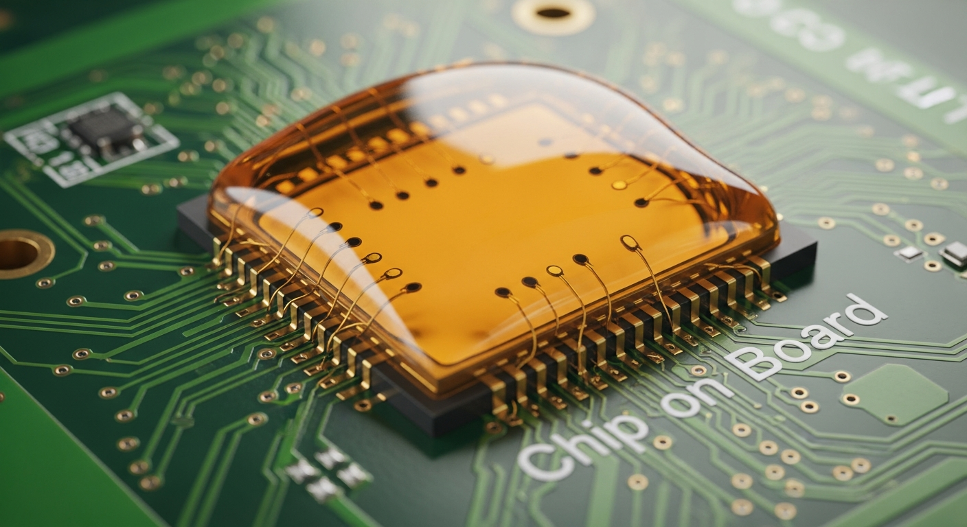
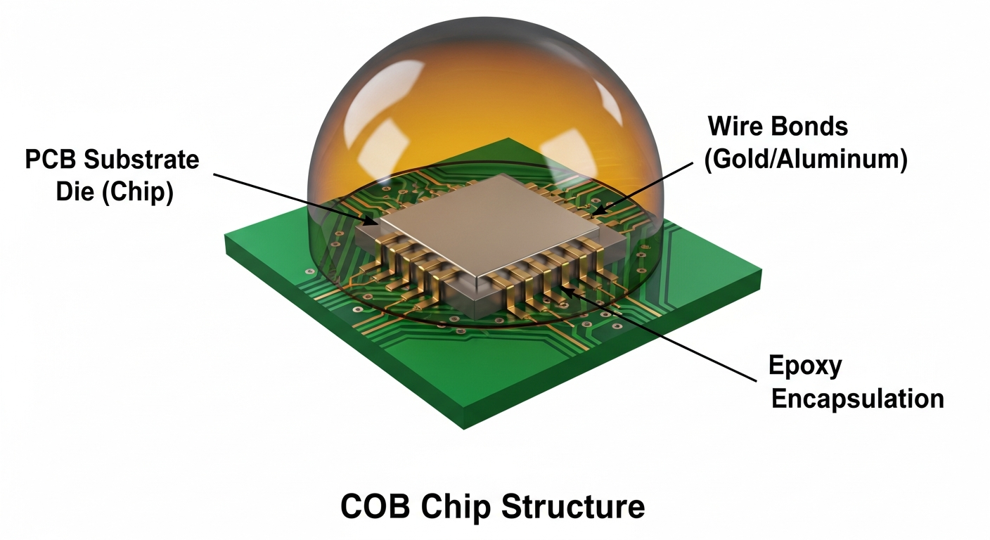
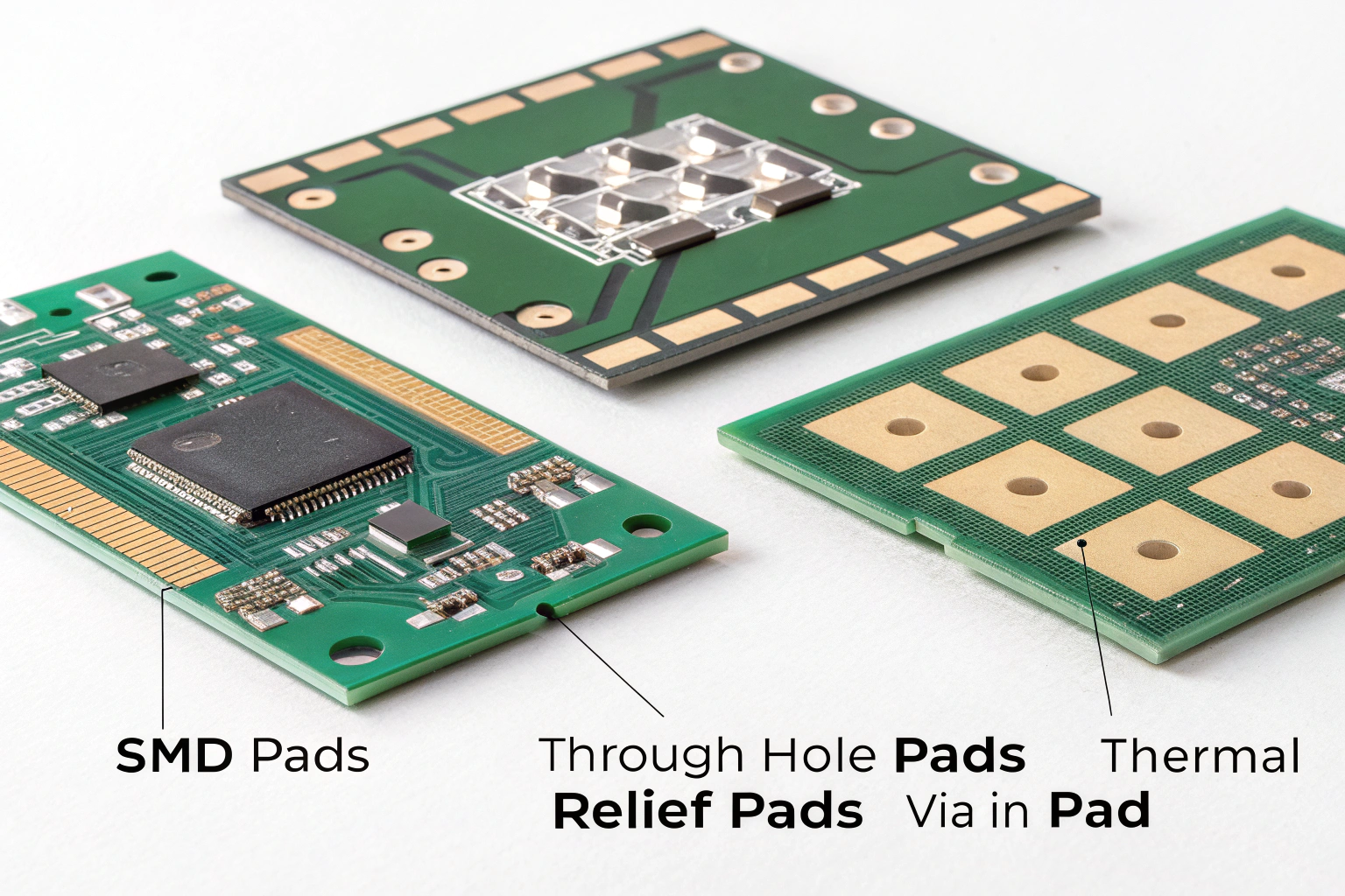
Chip on Board (COB) is a packaging method where bare semiconductor dies are directly mounted and wire-bonded on a PCB, then sealed with epoxy. It reduces size, cost, and improves thermal performance for compact electronics.
COB technology is widely used in LED lighting, smart sensors, wearables, and low-cost consumer devices. It minimizes packaging layers and enables extremely compact layouts. Many high-volume electronics rely on COB for stable performance under limited space and tight budgets.
What is a Chip On Board?
COB integrates a bare die directly onto the substrate, eliminating conventional chip packages.
COB works by attaching an unpackaged semiconductor die to a PCB, bonding it with gold or aluminum wires, and encapsulating it with epoxy for protection.
The method bypasses traditional IC packaging steps such as plastic molding or lead frame formation. Instead, the PCB becomes the carrier. This shortens the electrical path, improves heat transfer, and reduces per-unit cost, especially in high-volume products.
How COB is constructed
- Die attach – The bare die is glued or soldered onto the PCB.
- Wire bonding – Gold, aluminum, or copper wires connect the die pads to PCB traces.
- Encapsulation – Epoxy resin (transparent or black) protects the die and bonds.
- Testing – Functional tests verify bonding integrity and electrical operation.
Industry relevance
COB remains essential in compact electronics where board area, thermal control, and cost per unit influence design choices. LED manufacturers and IoT device makers use COB platforms to achieve dense layouts without expensive IC packages.
What are the main applications of Chip On Board?
COB supports many industries due to its compact size and cost efficiency.
COB is commonly used in LED modules, IoT sensors, medical devices, smart wearables, calculators, toys, and low-power consumer electronics.
COB shines in products that require small footprints or sealed structures. With LEDs, COB technology creates uniform, high-density arrays with excellent thermal performance. In sensors, the method integrates bare dies directly into compact housings or flexible substrates.
Key application areas
LED lighting
COB LEDs deliver high brightness, uniform light output, and good thermal conduction.
Consumer electronics
Keyboards, remote controls, calculators, and toys use black epoxy COB blobs to reduce cost.
IoT modules
Small sensors, beacons, and low-energy nodes benefit from compact die integration.
Medical and wearable devices
COB enables lightweight, miniaturized products with high signal accuracy.
Industrial control modules
High-density signal processing circuits use COB to minimize package overhead.
The technique allows manufacturers to reduce cost while increasing integration density.
What packaging techniques are used in Chip On Board?
COB includes multiple process steps related to bonding, coating, and substrate design.
Common COB packaging methods include gold wire bonding, aluminum wedge bonding, epoxy encapsulation, and thermal-optimized PCB layouts.
Industrial COB packaging requires controlled humidity, cleanroom environments, and precise bonding equipment. This ensures consistent electrical performance and protection against mechanical or chemical damage.
Core process elements
Die attach materials
Silver epoxy, conductive glue, or solder paste ensure thermal conduction.
Wire bonding
- Gold ball bonding for high precision
- Aluminum wedge bonding for power devices
- Copper bonding for cost-sensitive production
Encapsulation
Transparent epoxy for LEDs
Black epoxy for logic circuits and consumer applications
Substrate design
FR4, aluminum substrates, ceramics, and flexible PCBs serve different thermal and mechanical needs.
Manufacturers use IPC-compliant inspection methods (AOI, X-ray, electrical tests) to verify strong wire bonds and defect-free encapsulation.
What are the advantages of COB compared to traditional IC packaging?
COB removes several packaging layers, making devices simpler and smaller.
COB offers lower cost, smaller size, shorter interconnect paths, better thermal performance, and higher assembly flexibility compared to packaged ICs.
Because the bare die sits directly on the PCB, resistance and parasitic inductance decrease, improving signal integrity. This is valuable for LED drivers, audio modules, miniature sensors, and compact logic systems.
Main advantages
| Advantage | Description |
|---|---|
| Cost reduction | No plastic package, pins, or external housing |
| Space savings | Thinner, smaller footprint |
| Better heat performance | Direct thermal path into PCB substrate |
| High-density layouts | Multiple dies on one board |
| Process flexibility | Allows curved, flexible, or nonstandard shapes |
COB works especially well in mass-market products requiring low cost and compact form factors.
What are the limitations or risks of COB?
Despite its strengths, COB requires strict control and good manufacturing conditions.
**COB limitations include vulnerability to moisture, difficulty reworking, dependency on cleanroom processes, and lower mechanical protection compared to packaged ICs.
COB modules cannot be easily repaired once encapsulated. They also depend heavily on proper epoxy sealing to prevent corrosion or wire-bond failure. High-humidity deployments require protective coatings or sealed housings.
Key challenges
- Sensitive to contamination during bonding
- Requires precise alignment and controlled wire loop height
- Limited long-term mechanical strength without added protection
- Hard to perform field repairs
- Not ideal for high-power ICs unless substrates are optimized
Industries mitigate these constraints through conformal coating, better substrate materials, and stricter process validation.
How does COB compare to COF, COG, and other chip-level packaging?
COB belongs to a wider family of direct-attach technologies.
COB mounts the die on a PCB, while COF uses flexible film, and COG bonds the die directly onto glass substrates.
These variations serve different industries. COG dominates display drivers; COF supports foldable devices; COB fills the gap for cost-optimized logic and lighting modules.
Comparison table
| Packaging Type | Substrate | Typical Use | Advantages |
|---|---|---|---|
| COB | PCB | LEDs, sensors, toys | Low cost, small size |
| COF | Flexible film | Wearables, foldables | Ultra-thin, flexible |
| COG | Glass | LCD/OLED drivers | Minimal interconnect loss |
| POP | Stacked IC | High-performance CPUs | High integration |
Understanding these options helps designers choose the right technology based on mechanical, thermal, and cost constraints.
Conclusion
Chip on Board packaging remains one of the most efficient ways to integrate semiconductors into compact electronics. Its ability to mount bare dies directly on a PCB reduces material cost, improves thermal performance, and supports dense component layouts. COB thrives in LED lighting, IoT modules, wearables, sensors, and high-volume consumer products where small size and low price matter. Although it requires clean environments, precise bonding, and proper encapsulation, COB delivers reliable long-term performance when manufactured correctly. As electronics continue to shrink and integrate more features, COB will remain an essential technology for cost-driven industries that need stable, miniature, and scalable solutions across global markets.
