
A printed circuit board (PCB) is the physical foundation of almost all modern electronic devices. From industrial controllers and power systems to consumer electronics and medical equipment, PCBs provide both mechanical support and electrical connections for electronic components. Without PCBs, electronic products would be unstable, bulky, and unreliable.
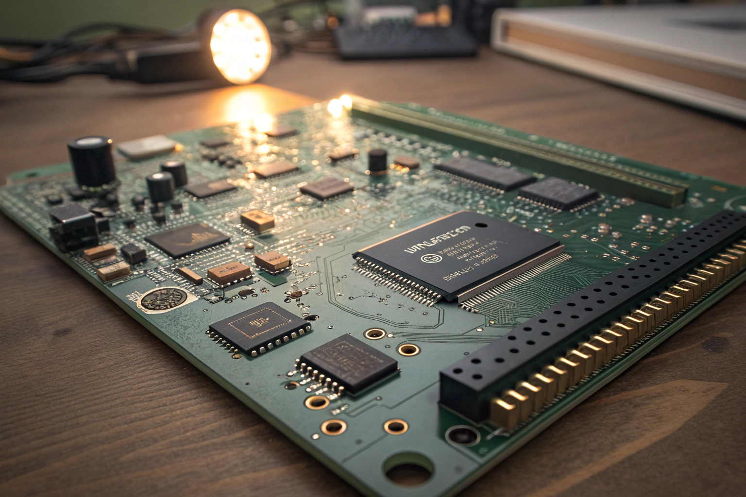
A PCB works by using copper traces etched onto an insulating board to connect electronic components electrically and mechanically. These copper paths replace traditional wiring, enabling stable signal transmission, compact layouts, and repeatable manufacturing for electronic assemblies.
To understand how a PCB works in real applications, it is important to explore its structure, materials, signal behavior, manufacturing process, and assembly methods. The following sections explain these topics from an engineering and manufacturing perspective.
What Are the Main Parts of a PCB?
A PCB is made up of several key elements that work together to form a functional circuit platform. Each part has a specific role in ensuring electrical performance and mechanical stability.
The main parts of a PCB include:
- Base material (substrate): Provides mechanical strength and insulation
- Copper layers: Form conductive paths for electrical signals
- Solder mask: Protects copper traces and prevents solder bridging
- Silkscreen: Marks component locations and identifiers
The most commonly used substrate material is FR4, a glass-fiber reinforced epoxy laminate. It offers a good balance of strength, insulation, and heat resistance. Copper layers are laminated onto the substrate and later patterned to create circuit traces. These traces act like roads that guide electrical current between components.
How Do Electrical Signals Flow on a PCB?
Electrical signals on a PCB travel through copper traces rather than loose wires. Each trace is designed with a specific width and spacing to handle current, voltage, and signal speed requirements.
Signals move from one component pin to another following the copper routing. In more complex designs, vias are used to move signals between different layers of the board. Vias are plated holes that provide vertical electrical connections.
Signal behavior depends on:
- Trace width and thickness
- Distance to reference planes
- Board material properties
- Operating frequency
As signal speeds increase, trace layout becomes more critical. Controlled impedance, short return paths, and proper grounding help maintain signal integrity and reduce noise or interference.
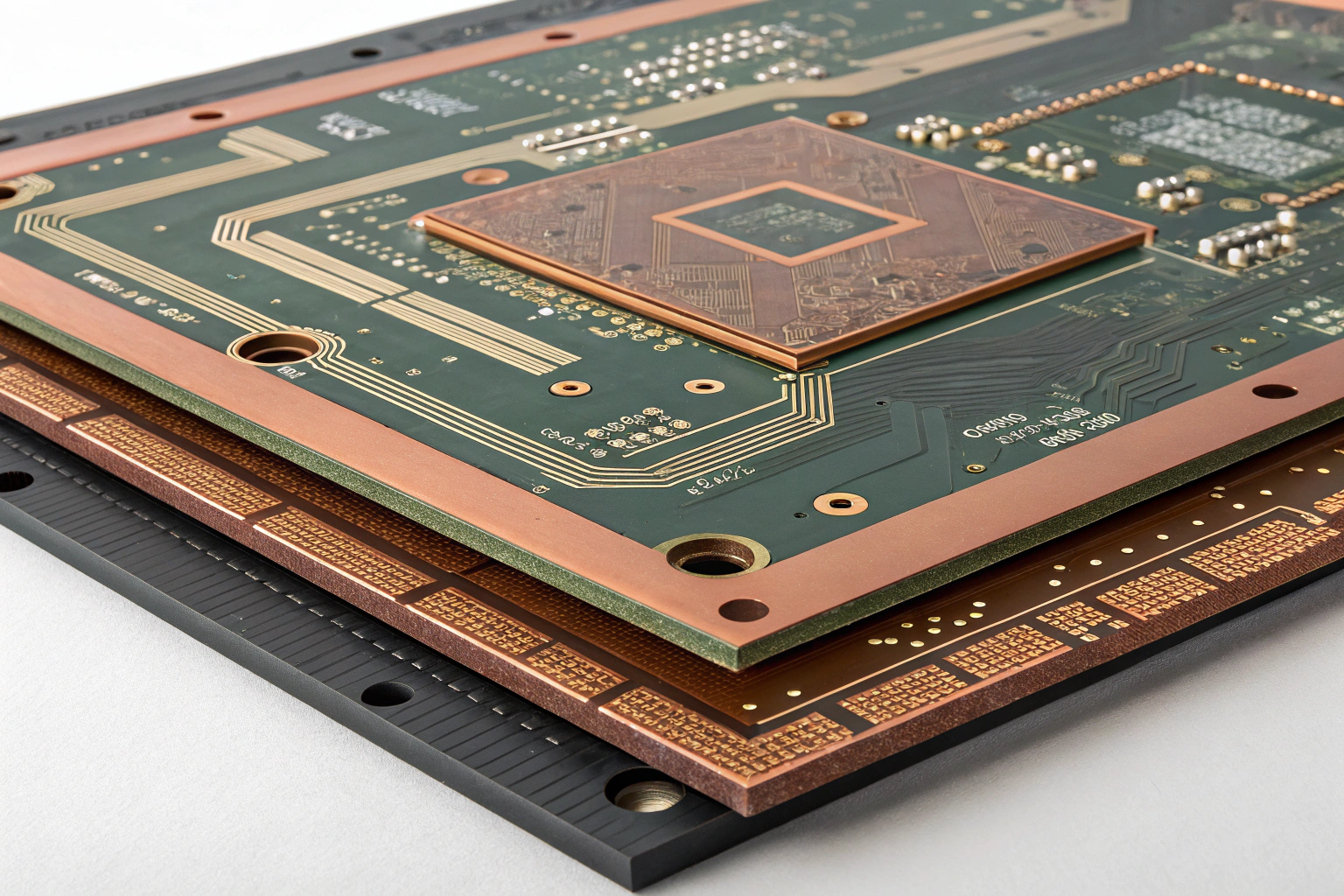
What Types of PCBs Are Commonly Used?
PCBs are classified based on the number of copper layers and structural complexity. Each type serves different product requirements.
Common PCB types include:
- Single-layer PCBs: One copper layer, simple and low cost
- Double-layer PCBs: Two copper layers with vias
- Multilayer PCBs: Multiple internal copper layers
- Flexible PCBs: Bendable circuits for compact designs
- Rigid-flex PCBs: Combined rigid and flexible sections
Multilayer PCBs are widely used in advanced electronics because they support higher component density and better signal control. Internal power and ground planes improve electrical stability and reduce electromagnetic interference.
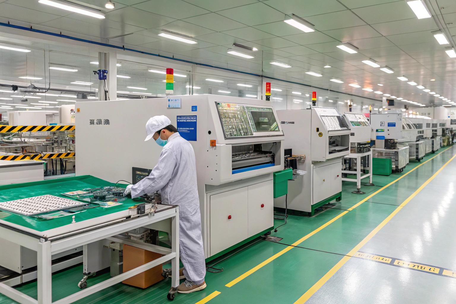
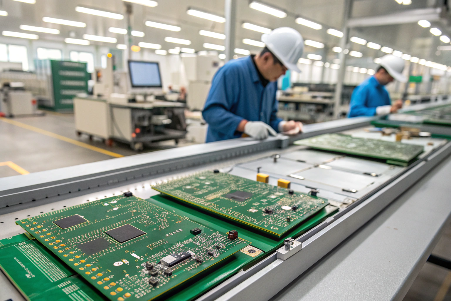
How Is a PCB Manufactured in the Factory?
PCB manufacturing is a precise and highly controlled process. It begins with converting design files into production data and ends with electrical testing.
The main manufacturing steps include:
- Cutting and cleaning raw laminate
- Copper imaging and etching
- Layer alignment and lamination (for multilayer boards)
- Drilling vias and component holes
- Copper plating and surface treatment
- Solder mask and silkscreen printing
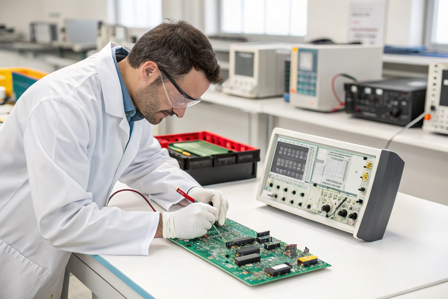
- Electrical testing and inspection
Factory workshops use automated equipment to ensure accuracy at every stage. Lamination pressure, drilling precision, and plating thickness are closely monitored. Inspection methods such as automated optical inspection and electrical testing help detect defects before assembly.
How Does PCBA Assembly Work?
Once the bare PCB is completed, electronic components are mounted through a process called PCB assembly (PCBA). This step transforms the board into a functional electronic unit.
Assembly methods include:
- Surface-mount technology (SMT): Components mounted directly onto pads
- Through-hole assembly: Leads inserted into drilled holes
- Mixed assembly: Combination of SMT and through-hole
Solder paste is printed onto pads, components are placed by machines, and the board passes through a reflow oven to form solder joints. After assembly, inspections such as AOI, X-ray, and functional testing ensure electrical performance and reliability.
Why Are PCBs Essential for Modern Electronics?
PCBs provide consistency, reliability, and scalability that manual wiring cannot achieve. They allow products to be smaller, lighter, and easier to mass-produce while maintaining stable electrical performance.
Key advantages of PCBs include:
- Compact circuit layout
- Repeatable manufacturing quality
- Improved signal stability
- Better thermal and mechanical control
As electronic systems grow more complex, PCB design and manufacturing become even more critical. Proper material selection, layout planning, and process control directly influence product lifespan and performance.
Conclusion
A PCB is far more than a simple board with copper lines. It is a carefully engineered platform that supports electrical connections, mechanical stability, and long-term reliability. By guiding electrical signals through designed copper paths and insulating layers, PCBs enable complex electronic systems to function accurately and efficiently.
From raw materials and copper patterning to factory manufacturing and final assembly, every stage contributes to the overall quality of the finished product. Poor control at any step can lead to signal instability, thermal stress, or early failure. For this reason, modern PCB production relies on standardized processes, strict inspections, and experienced engineering oversight.
As technology continues to advance toward higher speeds, smaller form factors, and increased integration, PCBs will remain the backbone of electronic innovation. A well-designed and well-manufactured PCB ensures that electronic products perform consistently, operate safely, and meet the demanding requirements of real-world applications over time.
