
An In-Depth Explanation of Printed Circuit Boards (PCBs)
Printed Circuit Boards (PCBs) are a crucial component in electronic devices, serving as the foundation for connecting electronic components in a unified circuit layout. This innovation eliminates the need for traditional point-to-point wiring, making circuit design and assembly more efficient and reliable. Components are soldered onto a board covered with conductive copper traces, which transmit current throughout the circuit.
The history of PCBs dates back to the late 19th century, but it wasn’t until the 1930s that their design and manufacturing technologies matured enough for practical applications. As technology advanced, especially in the 1950s and 1960s, PCBs became widespread and are now integral to nearly all electronic products that rely on complex internal circuits, such as smartphones, computers, and household appliances.
Modern PCB manufacturing employs semi-automated processes, significantly reducing the labor required compared to traditional point-to-point wiring while minimizing the risk of errors. This efficiency makes PCBs not only more cost-effective but also superior in terms of space utilization and electrical performance. Compared to other mass-produced circuit construction methods, PCBs offer a more convenient, economical, and reliable solution.
Moreover, as technology has evolved, the types and functionalities of PCBs have expanded. From single-sided boards to multi-layer boards, and from rigid boards to flexible ones, PCBs can accommodate various complex circuit needs. This versatility has led to their widespread application across multiple industries, including telecommunications, healthcare, automotive, and industrial equipment. Overall, the innovation and advancement of PCBs have not only driven the growth of the electronics industry but also play an increasingly important role in our daily lives.
Detailed Overview of PCB Manufacturing Process
The manufacturing of PCBs (Printed Circuit Boards) is a complex and professional process that encompasses multiple key stages from design to production. Here are the main steps and relevant details in PCB manufacturing:
1. Design Phase
In the PCB design phase, engineers use specialized Electronic Design Automation (EDA) software to create circuit schematics and PCB layouts. This stage includes:
- Circuit Schematic Design: Designers draw the circuit diagram, defining the connections between components to ensure that the circuit meets functional and performance requirements.
- PCB Layout Design: The circuit diagram is translated into a PCB layout, optimizing the placement of components and routing, while considering signal integrity, power distribution, and heat dissipation.
Once the design is completed, simulations are often conducted to validate the circuit’s functionality and performance.
2. Material Preparation
The materials needed for PCB manufacturing include:
- Substrate Material: Typically glass fiber (FR-4) or polyimide (PI), which have good electrical properties and mechanical strength.
- Conductive Material: Primarily copper foil, used to form the circuit traces.
- Insulating Material: Such as epoxy resin, used to isolate the circuit layers.
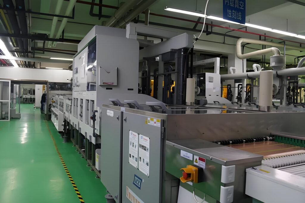
3. Manufacturing Process
The PCB manufacturing process typically includes several key steps:
- Printing Circuit Patterns: Using photolithography, the circuit design is transferred onto a substrate covered with a photosensitive coating. Through exposure and development, the circuit pattern is formed.
- Etching: Chemical etching solutions remove the unprotected copper layers, leaving the desired circuit traces.
- Drilling: Holes are drilled into the PCB to facilitate the insertion and connection of components. These holes can be through-holes (THT) or blind/buried vias (for high-density designs).
4. Solder Mask and Silkscreen
- Solder Mask: A solder mask layer is applied to protect the circuit and prevent solder bridging. This is typically green or other colors.
- Silkscreen: Identification and component numbers are printed on the PCB for assembly and maintenance purposes.
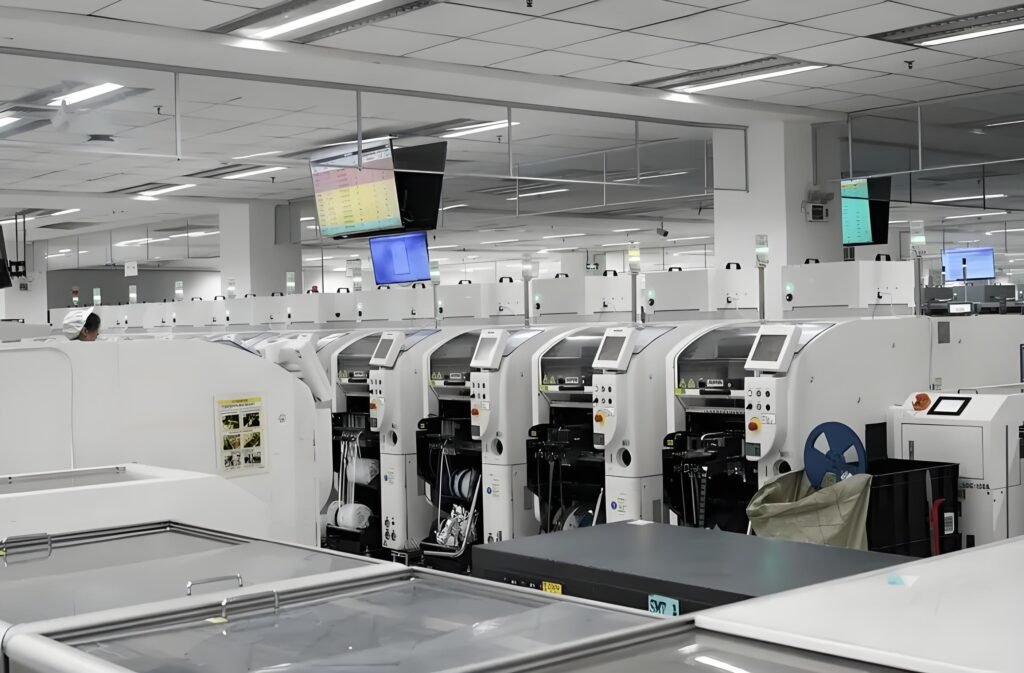
5. Component Assembly
- Surface Mount Technology (SMT): Surface-mounted components are soldered onto the PCB surface, typically using automated pick-and-place machines.
- Through-Hole Technology (THT): Component leads are inserted into the holes of the PCB, then secured through wave soldering or manual soldering.
6. Testing and Inspection
After the PCB assembly is complete, a series of tests are performed to ensure functionality. These tests may include:
- Visual Inspection: Checking solder joint quality and correct component placement.
- Functional Testing: Verifying the PCB’s performance in actual applications.
- Automated Optical Inspection (AOI): Using machines to perform automated checks on solder joints and traces, ensuring quality.
7. Packaging and Delivery
Once all tests and inspections are completed, the PCBs are cleaned and packaged, ready for delivery to customers. Depending on requirements, PCBs can be single-sided, double-sided, or multi-layered, suitable for various electronic devices.
The PCB manufacturing process involves multiple technical stages, each requiring precise control and rigorous inspection to ensure the quality and reliability of the final product. As the functionality and complexity of electronic products increase, PCB manufacturing technologies continue to advance to meet market demands. By optimizing design, material selection, and manufacturing processes, PCBs play an increasingly important role in a wide range of devices, driving rapid growth in the entire electronics industry.
PCB Application Field
PCBs are widely used across various fields, and their importance cannot be overstated. The main application areas include:
- Consumer Electronics: In devices such as smartphones, tablets, and household appliances, PCBs are core components of their internal circuits.
- Industrial Equipment: In automation control systems, instrumentation, and electrical devices, PCBs perform complex electrical connections and signal transmission tasks.
- Automotive Electronics: Modern vehicles are equipped with numerous electronic components, and PCBs are used in automotive control systems, navigation devices, and safety systems.
- Medical Devices: In medical instruments, PCBs ensure precise signal processing and reliable performance, involving monitoring devices and diagnostic instruments.
2. PCB Manufacturing Process
The PCB manufacturing process is complex and typically involves the following key steps:
- Pattern Transfer: Using photolithography to transfer the design pattern onto the copper foil. This step is crucial for ensuring the accuracy of the circuit.
- Etching: Removing excess copper layers through chemical etching, leaving only the necessary conductive pathways.
- Laminating: Combining different layers of PCB materials to create multilayer circuit boards, ensuring the integrity and stability of the circuits.
- Testing: Each PCB undergoes electrical testing before leaving the factory to confirm its functionality and reliability, reducing the occurrence of future failures.
3. PCB Maintenance and Care
Regular maintenance and care are essential to extend the lifespan of PCBs. The main measures include:
- Regular Inspections: Periodically checking the electrical connections, solder joints, and physical condition of the PCB to detect and repair potential issues promptly.
- Moisture Control: Storing PCBs in dry environments to prevent moisture-induced short circuits and corrosion.
- Static Protection: Implementing static protection measures when handling PCBs to avoid damage caused by electrostatic discharge.
- Cleaning: Regularly cleaning the PCB surface to remove dust and dirt, ensuring optimal electrical performance.
By implementing these measures, the reliability and lifespan of PCBs can be effectively enhanced.
What Other PCB Services Might You Need?

At CustomPCBA, we provide a comprehensive range of PCB services tailored to meet the diverse needs of our clients. Here are some of our specialized service areas:
1. Blank PCB Production
Whether you need one-time prototypes, small batch production, or large-scale orders, we offer blank PCBs with various material thicknesses, copper weights, and solder mask colors. Clients can flexibly choose based on specific project requirements to ensure optimal circuit performance.
2. PCB Design Services
Our professional CAD design team utilizes advanced design software to accurately convert your circuit diagrams and technical specifications into manufacturable PCB designs. We focus on design for manufacturability, ensuring that high-quality products can be achieved during production.
3. Rapid PCB Prototyping
We are renowned for our PCB prototyping services, capable of manufacturing, quality-checking, and delivering prototype boards in an extremely short time frame. Our efficient processes ensure that clients can quickly validate their products and conduct market testing.
4. PCB Manufacturing Solutions
We specialize in providing high-precision PCB manufacturing and production control services, committed to ensuring that every product meets stringent quality standards. Whether it’s single-layer, double-layer, or multi-layer PCBs, we have the capability to meet diverse design requirements.
5. PCB Assembly Services
We offer comprehensive PCB assembly services that cover the entire process from component sourcing to precise installation. Whether using components provided by us or those supplied by the client, we guarantee quality and efficiency in assembly.
6. PCB Reverse Engineering
Our reverse engineering services assist clients in recreating or improving existing circuit designs to enhance cost-effectiveness and efficiency. We possess deep technical knowledge and experience, enabling us to effectively analyze and replicate complex circuit boards.
7. Flexible PCB Solutions
For specialized equipment or specific applications, we can design and manufacture robust flexible PCBs on flexible plastic substrates. This design offers greater flexibility and adaptability, making it particularly suitable for tight spaces or dynamic applications.
Through these comprehensive services, CustomPCBA aims to provide clients with full support from design to production, ensuring that every project proceeds smoothly and achieves optimal results.
Custompcba’s Complete PCB solution
At CustomPCBA, we offer comprehensive end-to-end PCB services to meet a wide range of design and performance requirements. Whether you need us to be involved throughout the entire process or just handle specific stages of PCB design, prototyping, manufacturing, and assembly, we are here to provide professional support.
With nearly forty years of experience in the printed circuit board engineering field, we have established an outstanding reputation. We are not only dedicated to delivering precise technical services but are also known for our industry-leading turnaround times. We adhere strictly to confidentiality agreements, earning the trust of a loyal clientele who consistently rely on us to develop proprietary circuits under these conditions.
Moreover, we take pride in our ability to deliver flawless results every time. Our customer satisfaction guarantee reflects our confidence in the accuracy of our work and our team’s meticulous attention to detail.
If you would like to discuss any aspects of your upcoming PCB production project with a member of the CustomPCBA team, please feel free to contact us by phone or email. We look forward to supporting your project and ensuring exceptional outcomes.
