
A Type 3 PCB refers to a multilayer printed circuit board with four or more conductive layers. It is commonly used in applications that require higher circuit density, better signal control, and improved electrical performance compared to single-layer or double-layer boards.
In manufacturing, Type 3 PCBs represent a key transition point from basic boards to more complex multilayer structures. The process involves advanced materials, tighter process control, and higher demands on factory equipment and engineering capability.
How is a Type 3 PCB different from other PCB types?
PCB types are often classified by layer count. Type 1 PCBs are single-layer boards, while Type 2 PCBs are double-layer boards. Type 3 PCBs include four layers or more, introducing internal signal and plane layers.
This added complexity allows Type 3 PCBs to support denser routing, dedicated ground and power planes, and improved electromagnetic performance. Internal layers reduce noise, improve impedance stability, and support higher-speed signals.
From a manufacturing perspective, Type 3 PCBs require lamination, precise layer alignment, and controlled drilling and plating processes. These requirements distinguish them from simpler PCB structures and demand a more mature production environment.
What are the typical structures of a Type 3 PCB?
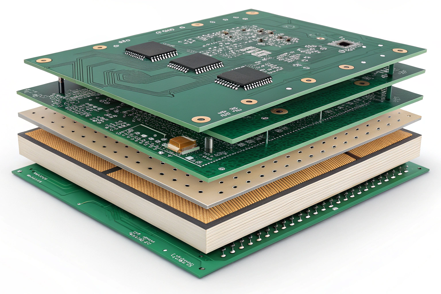
A common Type 3 PCB structure includes four layers: top signal layer, internal ground plane, internal power or signal layer, and bottom signal layer. Variations exist depending on electrical and mechanical requirements.
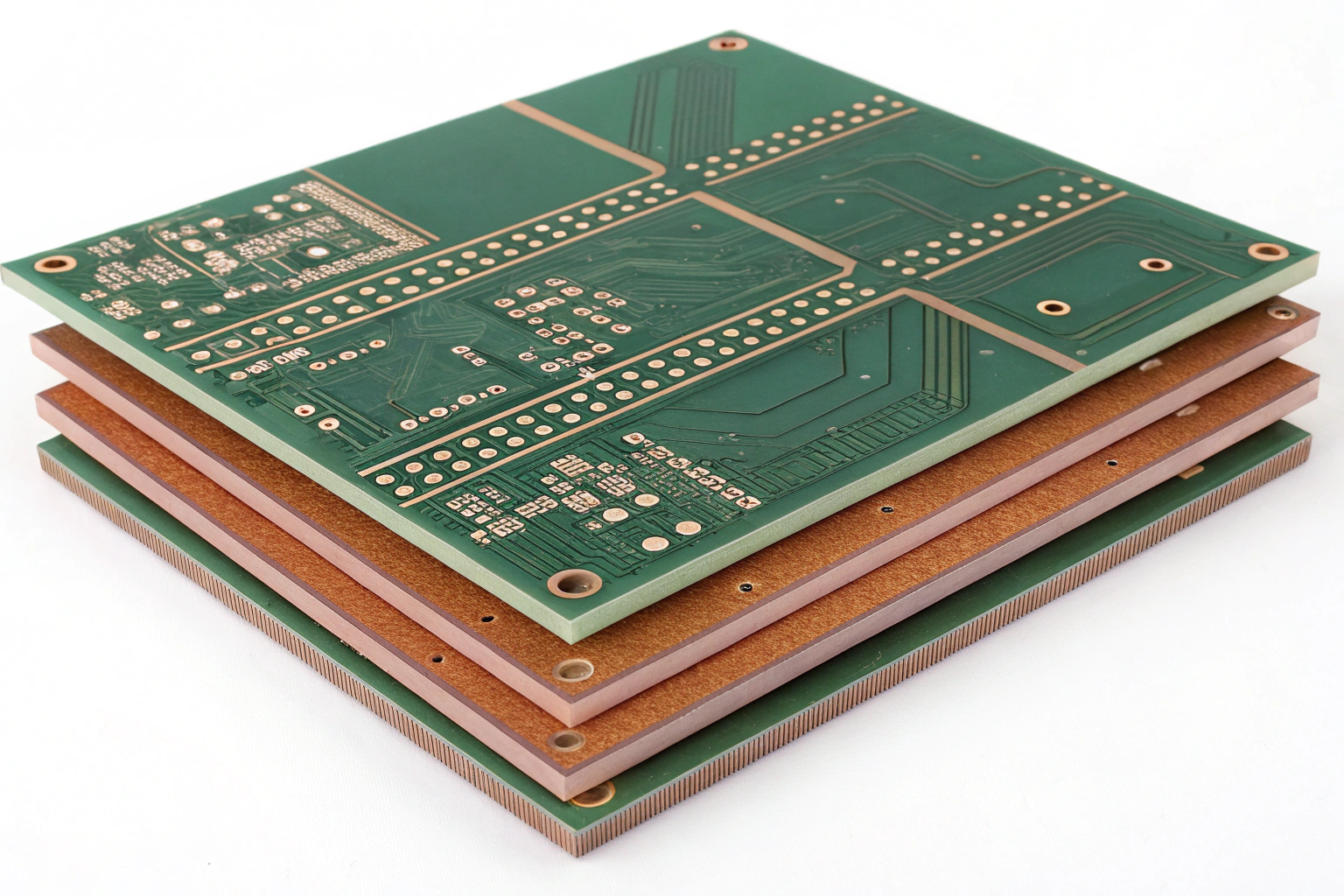
The internal planes provide stable reference paths for signals, reducing impedance fluctuations and electromagnetic interference. This structure is especially important for control systems, communication boards, and mixed-signal designs.
In factory production, stack-up design directly affects lamination pressure, prepreg selection, and thermal behavior. Accurate stack-up control ensures consistent thickness, reliable vias, and predictable electrical performance across production batches.
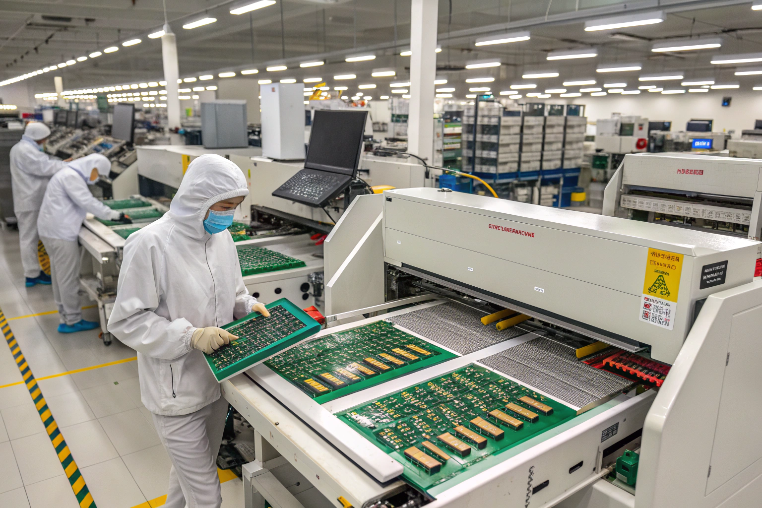
How is a Type 3 PCB manufactured in the factory?
Type 3 PCB manufacturing involves multiple controlled stages beyond basic etching.
Production begins with inner layer processing. Copper patterns are imaged and etched on inner cores, followed by optical inspection. Approved inner layers are stacked with prepreg and copper foil, then laminated under high temperature and pressure.
After lamination, CNC drilling creates vias and through holes. These holes are then metallized using electroless and electroplating processes to establish interlayer connections.
Outer layer imaging, etching, solder mask application, surface finishing, and silkscreen printing follow. Each step requires strict parameter control to maintain alignment and reliability. A factory equipped with multilayer lamination presses, high-precision drills, and advanced inspection systems is essential for stable Type 3 PCB production.
What manufacturing challenges are associated with Type 3 PCBs?
Compared with simpler boards, Type 3 PCBs present several production challenges.
Layer registration is critical. Even small misalignments can cause via breakout or signal integrity issues. Drilling accuracy must match plating capability to ensure reliable interconnections.
Thermal stress during lamination and soldering is another concern. Improper material selection or process control can lead to delamination or warping.
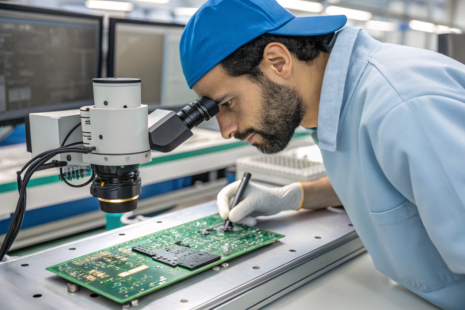
To address these risks, professional manufacturers rely on controlled material storage, process monitoring, and in-process inspections. Engineering teams continuously adjust lamination profiles, drill parameters, and plating thickness to match board complexity.
Where are Type 3 PCBs commonly used?
Type 3 PCBs are widely used in products that require stable electrical performance and compact design.
Typical applications include industrial control boards, communication equipment, power management modules, medical electronics, and advanced consumer devices. These products often operate under continuous load or harsh environments, demanding higher reliability.
In these applications, the internal planes of Type 3 PCBs improve noise immunity and power distribution. This contributes to stable operation and longer service life, which are key performance indicators for complex electronic systems.
How do factory capabilities affect Type 3 PCB quality?
The quality of a Type 3 PCB is closely tied to factory capability and process maturity.
Manufacturers with in-house multilayer production lines can control every step, from inner layer imaging to final electrical testing. Workshop layout, clean production environments, and disciplined process flow reduce contamination and handling damage.
Engineering involvement throughout production ensures that design intent is accurately translated into physical boards. Detailed production records and testing data support traceability and consistency.
Strong factory control results in Type 3 PCBs with stable impedance, reliable vias, and uniform quality across different batches and product revisions.
Conclusion
Type 3 PCBs represent a critical level in PCB manufacturing, combining multilayer structure with enhanced electrical performance. Their production requires advanced materials, precise lamination, accurate drilling, and disciplined process control.
When manufactured in a well-equipped factory with mature engineering and workshop management, Type 3 PCBs deliver reliable signal integrity, improved power distribution, and long-term stability. These characteristics make them a foundational choice for modern electronic products that demand performance, durability, and consistency over their entire lifecycle.
