
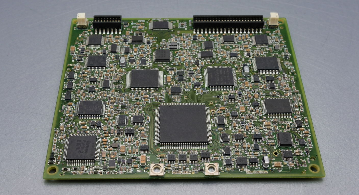
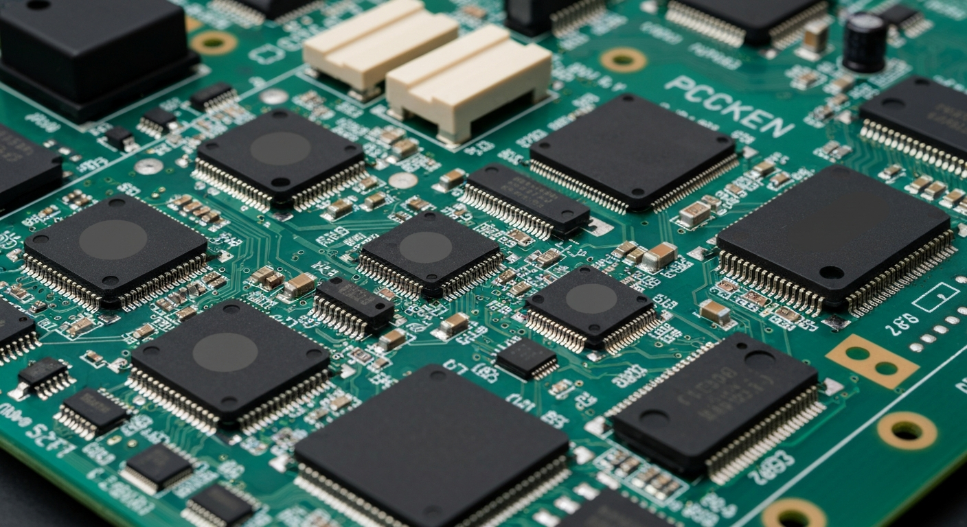
PCBA refers to a fully assembled printed circuit board that includes all components soldered and electrically connected. It is the finished, functional board used inside electronic products.
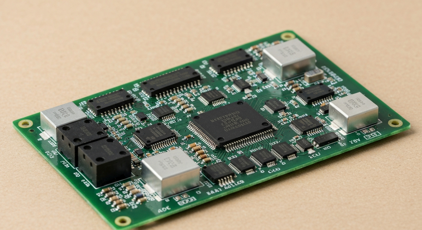
PCBA transforms a raw PCB into a complete electronic module. It becomes the core building block for smart devices, industrial systems, IoT hardware, and many other applications.
What is PCBA?
Many people confuse the bare board with the assembled board. PCBA explains the entire manufacturing journey from blank copper board to finished unit.
PCBA is the process and result of assembling components onto a PCB using SMT, DIP, soldering, inspection, and testing methods. It produces a ready-to-use electronic assembly.
Deeper Insight
PCBA begins with a bare PCB. Components from the BOM are placed using SMT machines or manual DIP assembly. Reflow or wave soldering completes the electrical bonding. After this, AOI, X-ray, ICT, and FCT verify whether the circuit performs as intended.
Manufacturers treat PCBA as a complete workflow that includes material sourcing, soldering parameters, reflow profiles, AOI logic, and quality documentation. For B2B customers producing IoT modules, controllers, or smart devices, PCBA is the stage where reliability becomes measurable. Factories with in-house SMT lines, engineering teams, and OEM/ODM experience can optimize BOMs, improve soldering stability, and reduce prototype revisions. This approach shortens development time and ensures that both prototypes and mass-production lots maintain consistent performance.
What is PCB and how does it differ from PCBA?
PCB is often mistaken for a finished functional board. It is only the starting point.
A PCB is a bare board made of copper and insulating material. PCBA is the completed assembly where all components are mounted and electrically connected.
Deeper Insight
A bare PCB contains copper traces, pads, vias, and the board structure itself. It has no electrical function until components are added. PCBA converts this blank board into a functional electronic circuit.
Here is a simple comparison:
| Item | PCB | PCBA |
|---|---|---|
| Components | None | Fully assembled |
| Function | No electrical behavior | Fully functional circuit |
| Process level | Manufacturing stage | Manufacturing + assembly + testing |
| Use case | Base for assembly | Final module for products |
| Complexity | Mechanical + electrical design | Complete electrical performance |
Factories treat these two stages differently. PCB fabrication focuses on copper thickness, drill accuracy, solder mask alignment, and impedance control. PCBA focuses on pick-and-place accuracy, solder quality, thermal control, and inspection. B2B buyers often require both processes under one roof to reduce lead time, avoid communication gaps, and improve engineering consistency. Integrated factories manage the transition from PCB to PCBA seamlessly, greatly reducing production risk.
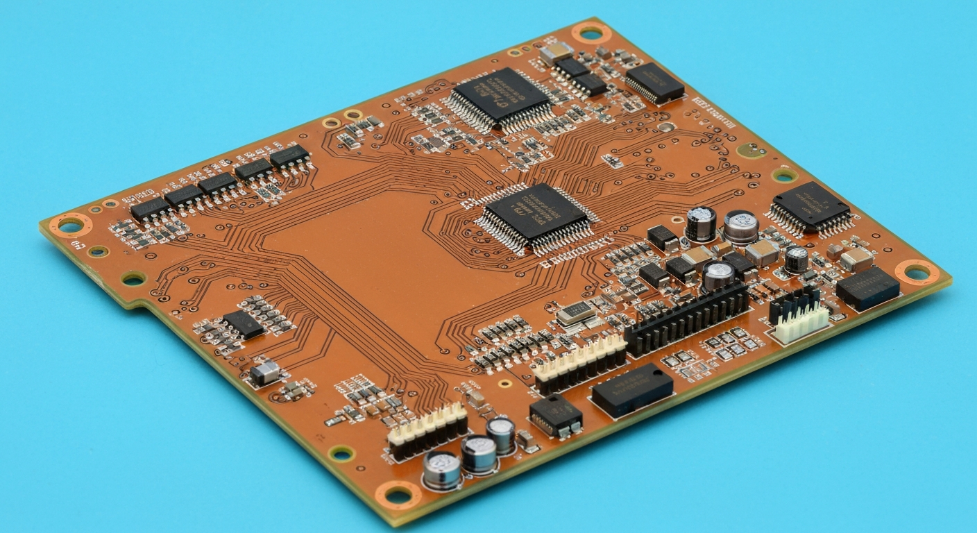
What are the benefits of using PCBA in modern electronics?
PCBA provides the essential electrical functionality that powers devices. It enables compact, complex, and reliable electronic systems.
Key benefits include faster prototyping, stable performance, smaller design footprint, and reduced assembly errors for final products.
Deeper Insight
PCBA technology allows designers to pack high-density circuits into small spaces. SMT placement enables fine-pitch ICs, BGAs, and 0201 components. Automation ensures consistent quality, and testing identifies issues early.
Benefits include:
Higher Reliability:
Automated assembly ensures stable solder joints and minimizes human error.
Faster Time to Market:
SMT lines complete complex assemblies within minutes, enabling rapid prototyping cycles.
Lower Labor Costs:
Automation reduces the need for manual soldering and rework.
Better Electrical Performance:
Controlled reflow curves improve joint integrity and reduce intermittent failures.
Scalable Production:
PCBA supports both small-batch builds and high-volume manufacturing.
B2B customers building industrial controllers, smart home modules, or communication devices rely on PCBA to turn ideas into products. Factories with complete PCBA capabilities offer BOM sourcing, engineering review, and testing, which removes bottlenecks and creates stable long-term supply chains.
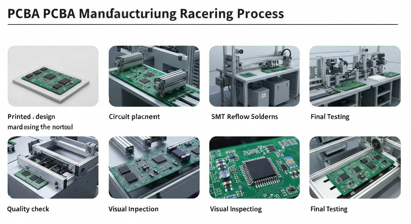
What is included in the PCBA manufacturing process?
PCBA is not a single step. It is a complete manufacturing workflow.
The PCBA process includes SMT printing, component placement, reflow soldering, DIP soldering, AOI inspection, testing, cleaning, and packaging.
Deeper Insight
A full PCBA workflow includes:
- Gerber + BOM review
- Stencil preparation
- Solder paste printing
- SMT pick-and-place
- Reflow soldering
- DIP insertion and wave soldering
- AOI and X-ray inspection
- ICT / FCT functional testing
- Cleaning and coating (optional)
- Packaging and labeling
Each stage affects electrical stability. For example, insufficient solder paste may cause open circuits, while uneven reflow profiles cause BGA voids. Integrated factories provide DFM checks to identify risks early, including pad design issues, wrong footprint sizes, or incorrect polarity markings.
Companies with in-house engineering teams support material alternatives, redesign hints, and yield improvements. For startups and industrial buyers needing small-batch builds, reliable PCBA processes prevent project delays and reduce rework costs.
Why choose PCBA instead of DIY assembly?
Modern components cannot be soldered reliably by hand, especially BGA, QFN, and 0201 packages.
PCBA offers machine precision, controlled thermal profiles, and comprehensive quality assurance—making it the only practical solution for high-quality electronics.
Deeper Insight
Hand-soldering may work for simple prototypes, but advanced circuits require:
- Correct solder paste volume
- Controlled reflow temperature curve
- Precise placement accuracy
- Inspection systems to detect hidden defects
Machines achieve these conditions consistently. For B2B customers, PCBA avoids defects such as bridging, tombstoning, cold joints, or insufficient solder. It also ensures predictable behavior for high-speed signals, RF circuits, and power modules.
Factories offering OEM/ODM services help customers transition from prototype to mass production smoothly. Engineering teams optimize BOMs, test procedures, and production documentation, creating a scalable pipeline that supports future product growth.
Conclusion
PCBA is the complete manufacturing process that transforms a bare PCB into a functional electronic module. It includes assembly, soldering, inspection, and testing—all essential for reliable product performance. By understanding the difference between PCB and PCBA, and recognizing the benefits of automated assembly, businesses can build stronger, more stable products with faster development cycles. A well-executed PCBA workflow supports long-term reliability, reduces engineering risk, and provides a dependable foundation for scaling from prototypes to mass production.
