
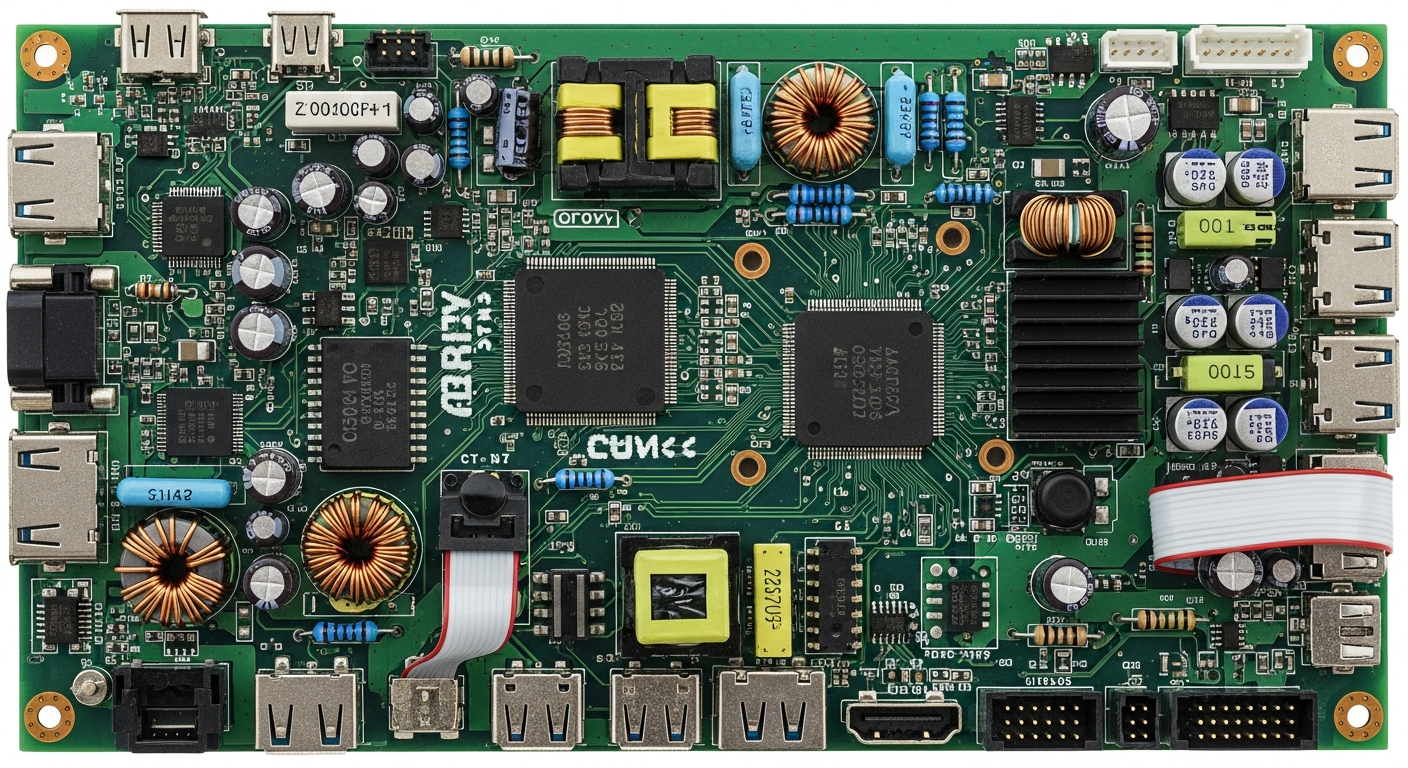
The PCBA manufacturing process follows a clear and controlled flow, starting from engineering review and material preparation, then moving through SMT, soldering, inspection, testing, assembly, and final delivery. Each step is tightly connected and directly affects product quality, reliability, and production efficiency.
The full process is not only about assembling components onto a PCB. It is a system that combines engineering judgment, standardized shop-floor operations, process control, and quality management. For manufacturers with in-house SMT workshops and engineering teams, this flow becomes a core competitive advantage, especially for complex boards and high-reliability applications.
How does engineering review and DFM analysis start the PCBA process?
Production risks often begin before manufacturing starts. Design issues, unclear files, or unsuitable footprints can cause delays and defects if not addressed early.
The PCBA process always starts with engineering review and DFM (Design for Manufacturability) analysis. Gerber files, BOM lists, assembly drawings, and test requirements are carefully checked to ensure they are complete and manufacturable.
During this stage, engineers focus on solder pad design, component packages, polarity markings, panelization methods, and process compatibility. For example, fine-pitch QFN or BGA devices require precise stencil design and placement accuracy. Connectors and tall components must be reviewed for reflow shadowing risks.
From a manufacturing perspective, this step directly links design decisions to shop-floor execution. A factory with its own engineering team can quickly adjust stencil openings, recommend footprint changes, or optimize panel layouts. This reduces rework and avoids trial-and-error during production.
In modern SMT workshops, DFM feedback is also connected to material availability and process capability. If certain components face supply risks, alternative part suggestions can be proposed before purchasing starts. This early intervention shortens lead time and stabilizes the entire production flow.
Why is PCB fabrication and incoming material control critical?
Unstable PCB quality or poor incoming materials can break the entire PCBA process, even if assembly is well controlled.
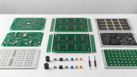
After design review, PCB fabrication and material preparation begin. Bare boards are produced according to layer count, material type, copper thickness, and surface finish. Common finishes include ENIG, HASL, and OSP, each affecting solderability and shelf life.
When PCBs arrive at the factory, incoming quality control is performed. This includes checking board thickness, surface condition, solder mask alignment, and hole quality. Warped or oxidized boards are rejected to prevent soldering defects later.
Electronic components also undergo incoming inspection. Packaging integrity, moisture sensitivity levels, and date codes are verified. Sensitive devices are stored in dry cabinets with humidity monitoring.
For manufacturers operating their own warehouses and SMT lines, material control is directly linked to production stability. Clear labeling, batch tracking, and FIFO management ensure that the correct parts are issued to each production order. This level of control supports consistency between prototypes and mass production.
How does SMT solder paste printing and placement work?
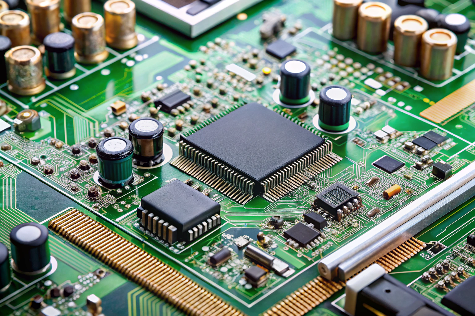
SMT is the core stage where most electronic components are mounted, and precision at this step defines final product quality.
The SMT process begins with solder paste printing. A stainless steel stencil is aligned with the PCB, and solder paste is evenly applied to each pad. Printing pressure, speed, and paste viscosity are carefully controlled.
After printing, SPI (Solder Paste Inspection) is often used to check paste volume and alignment. Insufficient or excessive paste can cause defects such as tombstoning or bridging.
Next comes component placement. High-speed pick-and-place machines mount resistors, capacitors, ICs, and connectors onto the solder paste. Placement accuracy is especially critical for 0201 components and fine-pitch packages.
In a professional SMT workshop, placement programs are optimized to balance speed and accuracy. Vision systems verify component orientation and polarity in real time. This reduces placement errors and improves first-pass yield.
For manufacturers with flexible production lines, SMT setups can be adjusted quickly for different board designs. This flexibility is important when handling mixed orders, prototypes, and small to medium batch production.
What happens during reflow soldering and process control?
Reflow soldering permanently bonds components to the PCB, and temperature control is the key factor.
Once components are placed, boards enter the reflow oven. The temperature profile is set according to solder paste type, PCB thickness, and component sensitivity. Typical stages include preheat, soak, reflow, and cooling.
If the profile is too aggressive, components may be damaged. If it is too weak, cold solder joints may form. Continuous monitoring ensures that each zone remains within the defined process window.
Process engineers regularly test and adjust profiles using thermal measurement tools. This ensures consistent solder quality across different batches and board types.
Factories with experienced process teams can quickly tune reflow settings for complex boards, such as multi-layer PCBs or boards with mixed thermal mass. This capability directly improves reliability and reduces hidden soldering defects.
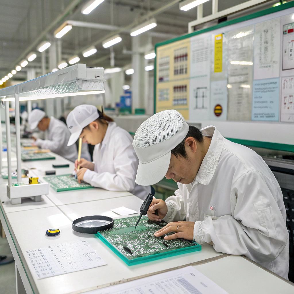
How are DIP soldering and mixed-technology assemblies handled?
Not all components are suitable for SMT. Connectors, transformers, and large capacitors often require through-hole assembly.
After SMT, boards move to the DIP and manual assembly area. Components are inserted into plated through holes, either manually or with selective insertion tools. Soldering is then completed using wave soldering or selective soldering machines.
Flux type, solder temperature, and conveyor speed are carefully controlled to avoid solder bridges or insufficient fill. Operators visually inspect joints and perform touch-up soldering if needed.
A factory with integrated SMT and DIP workshops can coordinate both processes smoothly. This reduces handling damage and ensures proper sequencing, especially for boards with both surface-mount and through-hole components.
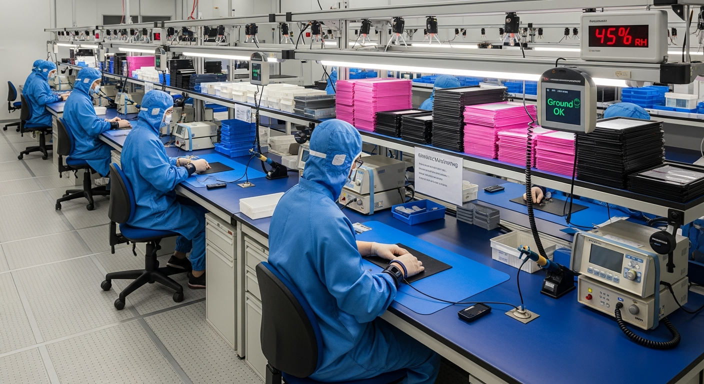
Why are AOI, ICT, and functional testing essential?
Assembly alone does not guarantee performance. Testing verifies that the board works as designed.
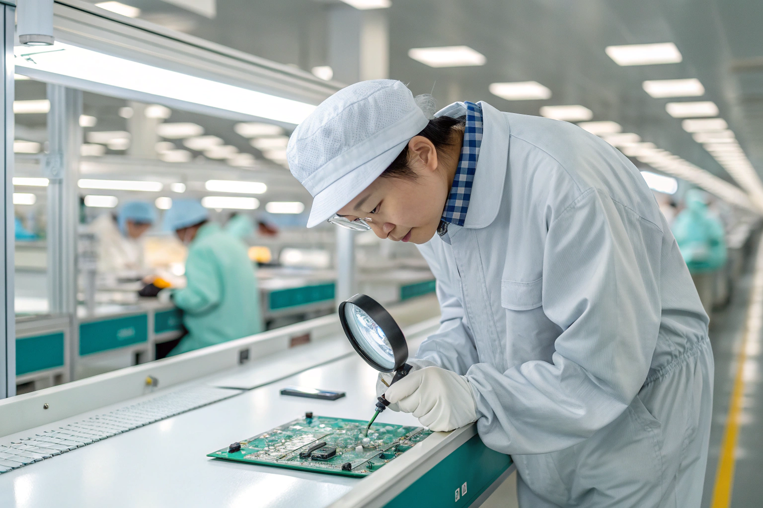
AOI (Automated Optical Inspection) checks solder joints, component placement, and polarity after SMT and DIP processes. It detects missing parts, misalignment, and solder defects.
For electrical verification, ICT (In-Circuit Test) measures resistance, continuity, and basic component values. Functional testing simulates real operating conditions to confirm that the board performs its intended function.
Test fixtures and procedures are developed based on product requirements. Factories with test engineering capabilities can customize test coverage and improve fault detection rates.
Strong testing systems reduce field failures and ensure stable performance across production batches.
How does final assembly, packaging, and quality assurance complete the flow?
The last stage ensures that the product is ready for real-world use and shipment.
After testing, boards may go through final assembly, such as enclosure installation, cable connection, or labeling. Cosmetic inspection ensures cleanliness and appearance standards are met.
Quality assurance teams review production records, inspection results, and test reports. Only boards that meet all criteria are approved for packaging.
Packaging methods are selected based on product sensitivity. Anti-static bags, vacuum sealing, and custom cartons protect boards during transportation and storage.
A manufacturer with full process ownership can maintain traceability from incoming materials to final shipment. This complete control supports consistent quality, faster problem resolution, and long-term product stability.
Conclusion
The PCBA manufacturing process is a structured flow that integrates engineering, materials, production, testing, and quality control. From early DFM review to final packaging, each step builds on the previous one. A factory with its own workshops, process control systems, and engineering teams can deliver stable quality, strong reliability, and efficient production across the entire lifecycle of electronic products.
