
Selecting the right PCB layer structure is a critical decision in electronic product development. As functional requirements increase, single or double layer boards often reach their practical limits in routing, electrical stability, and manufacturability. Multilayer PCBs are introduced to address these challenges in a systematic way.
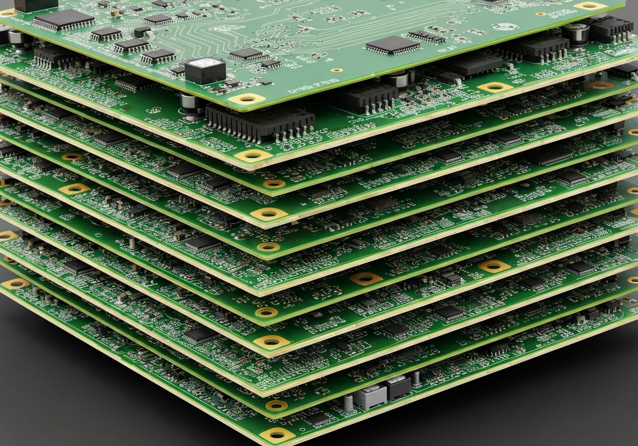
A multilayer PCB should be used when circuit complexity, signal integrity, power stability, EMI control, or size constraints exceed what single or double layer PCBs can reliably support.
In most cases, this transition starts at four layers.
The following sections outline the most common technical and manufacturing scenarios where multilayer PCBs become the appropriate choice.
When Routing Density Becomes Too High
Limited routing space forces structural changes.

As component count and pin density increase, routing all signals on one or two layers becomes inefficient. Traces become longer, narrower, and more congested, increasing noise and design risk.
Multilayer PCBs provide additional internal signal layers that:
- Shorten trace lengths
- Reduce routing congestion
- Improve layout clarity
From a manufacturing perspective, cleaner routing improves spacing control and etching accuracy, leading to higher yield and fewer layout-related defects.
When Signal Integrity Requirements Increase
High-speed signals need controlled environments.
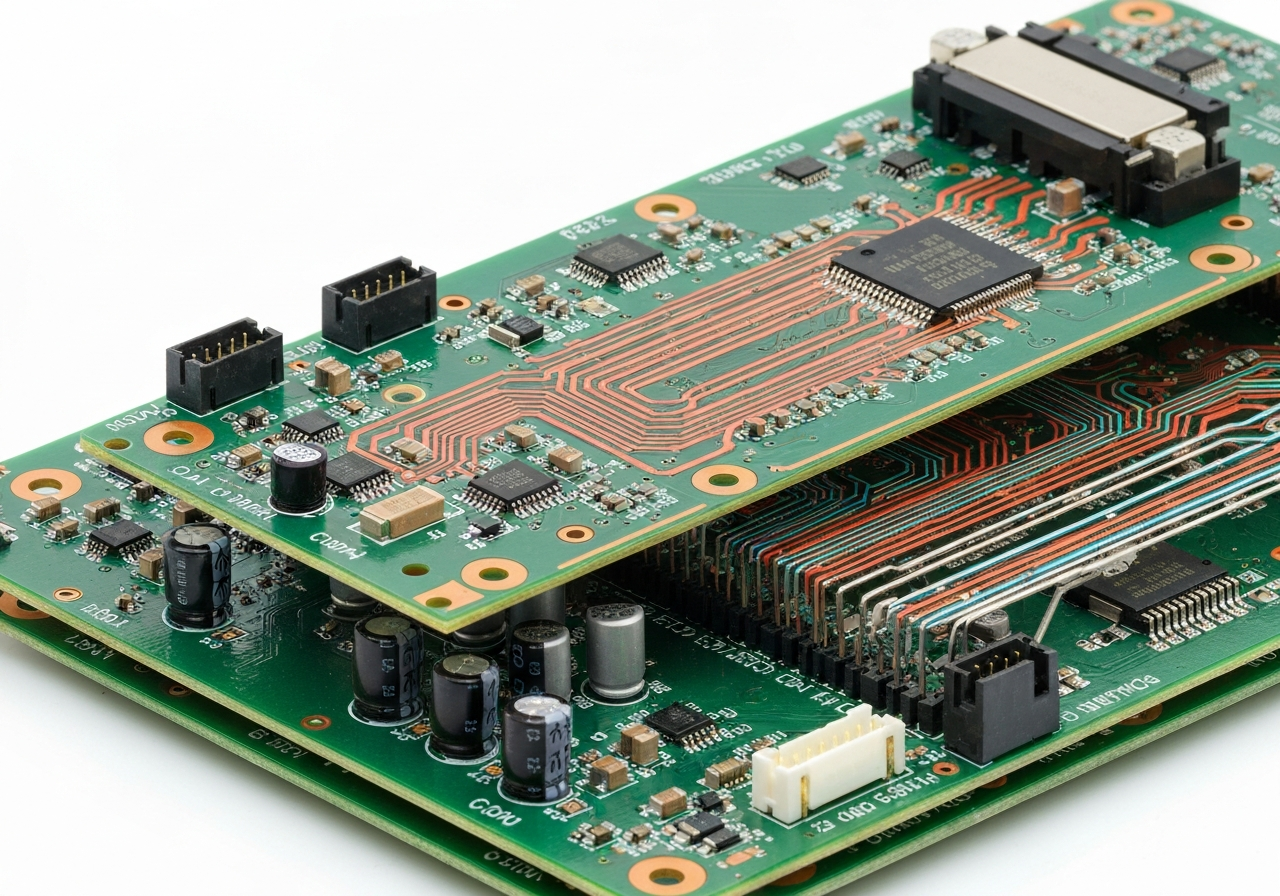
Fast digital interfaces, clocks, and communication lines are sensitive to impedance variation, crosstalk, and reflection.
Multilayer PCBs allow signal layers to be placed next to solid ground planes, providing stable return paths and controlled impedance. This structure produces more predictable electrical behavior across production batches and reduces functional variation during testing.
When Stable Power and Ground Distribution Is Required
Power quality affects the entire system.
Routing power and ground through narrow traces becomes unreliable as current demand increases.
Multilayer PCBs typically include dedicated power and ground planes that:
- Lower distribution impedance
- Reduce voltage drop
- Improve decoupling capacitor performance
- Suppress electrical noise
Boards with solid planes show fewer intermittent failures during factory testing and system-level validation.
When EMI and EMC Control Becomes Critical
Noise control often determines layer count.
Electromagnetic interference is commonly caused by long signal loops and poorly defined return paths.
Internal ground planes act as shields that contain electromagnetic fields and isolate noisy circuits from sensitive ones. Multilayer structures often resolve EMI issues that cannot be effectively addressed on two-layer boards without external shielding or layout compromises.
When Board Size Must Be Reduced
Vertical complexity enables compact design.
As product enclosures become smaller, fitting all circuitry onto a limited surface area becomes challenging.
Multilayer PCBs allow more routing to move inside the board, supporting tighter component placement and smaller outlines. In manufacturing, reduced board size can improve panel utilization and material efficiency.
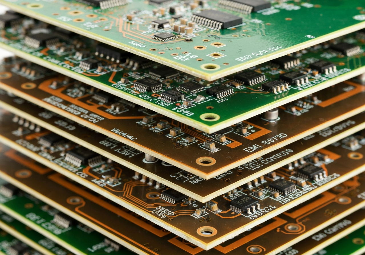
When Assembly Stability and Yield Matter
Manufacturing consistency becomes a priority.

Even-layer multilayer PCBs use symmetric stack-ups that distribute mechanical stress evenly.
In factory workshops, this leads to:
- Reduced warpage during reflow soldering
- Improved coplanarity for fine-pitch components
- More consistent solder joints
- Higher AOI and functional test pass rates
Stable assembly behavior is especially important for volume production and long-term quality control.
How Factory Processes Support the Decision to Use Multilayer PCBs
Process maturity reduces production risk.

Manufacturing multilayer PCBs involves controlled steps such as inner-layer imaging, lamination, drilling, plating, and inspection.
Standardized stack-ups and mature lamination recipes allow multilayer PCBs to be produced with predictable quality and repeatable results. Inner-layer AOI, via plating control, and electrical testing ensure internal layers perform as designed.
Conclusion
Multilayer PCBs should be used when electrical performance, routing density, power stability, EMI control, or size constraints exceed the practical limits of single or double layer boards. By separating signals, power, and ground into dedicated layers, multilayer structures provide a stable and predictable electrical environment.
From a manufacturing perspective, multilayer PCBs also deliver better assembly stability, higher yield, and more consistent quality when supported by mature factory processes. While they involve more complex fabrication steps, standardized stack-ups and controlled workshop procedures make multilayer PCBs an efficient and reliable solution for modern electronic products requiring scalability, stability, and long-term reliability.
