
Controlled impedance ensures that high-speed signals travel through a PCB with minimal distortion, reflection, or loss. Stable impedance improves signal integrity, EMC performance, and overall product reliability.
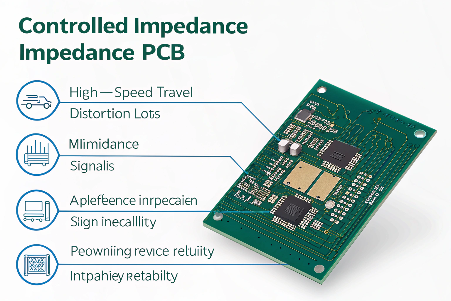
High-speed digital and RF circuits depend on predictable transmission paths. As rise times become faster and data rates increase, even short PCB traces behave like transmission lines. When impedance is not controlled, reflections, jitter, and eye-diagram collapse appear. Stable, engineered impedance is therefore essential for modern electronics.
What is controlled impedance in a PCB?
Controlled impedance refers to the engineered resistance of a signal trace to alternating current.
Controlled impedance is the target characteristic value of a PCB trace—typically 50Ω, 90Ω, or 100Ω—defined by its geometry, materials, and stack-up to ensure stable signal transmission.
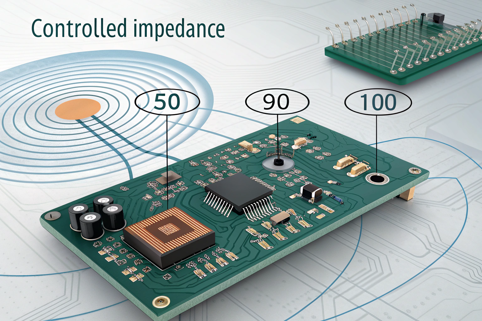
In high-speed systems, impedance depends on trace width, copper thickness, dielectric height, and the dielectric constant of the substrate. Manufacturers calculate these factors to match design specifications and maintain consistent behavior across all boards.
How impedance is defined
Controlled impedance involves electromagnetic field behavior. The copper trace forms part of a transmission line structure—microstrip, stripline, or dual-stripline. The dielectric material, usually FR4 or high-frequency laminate, sets how fields propagate. By tuning geometry, designers keep reflections low and maintain clean signal integrity.
Why manufacturers enforce it
Impedance accuracy ensures that every board performs identically. Production lines use impedance coupons, TDR testing, and strict stack-up control to maintain repeatable results for each layer and trace type.
Why does controlled impedance matter for high-speed signals?
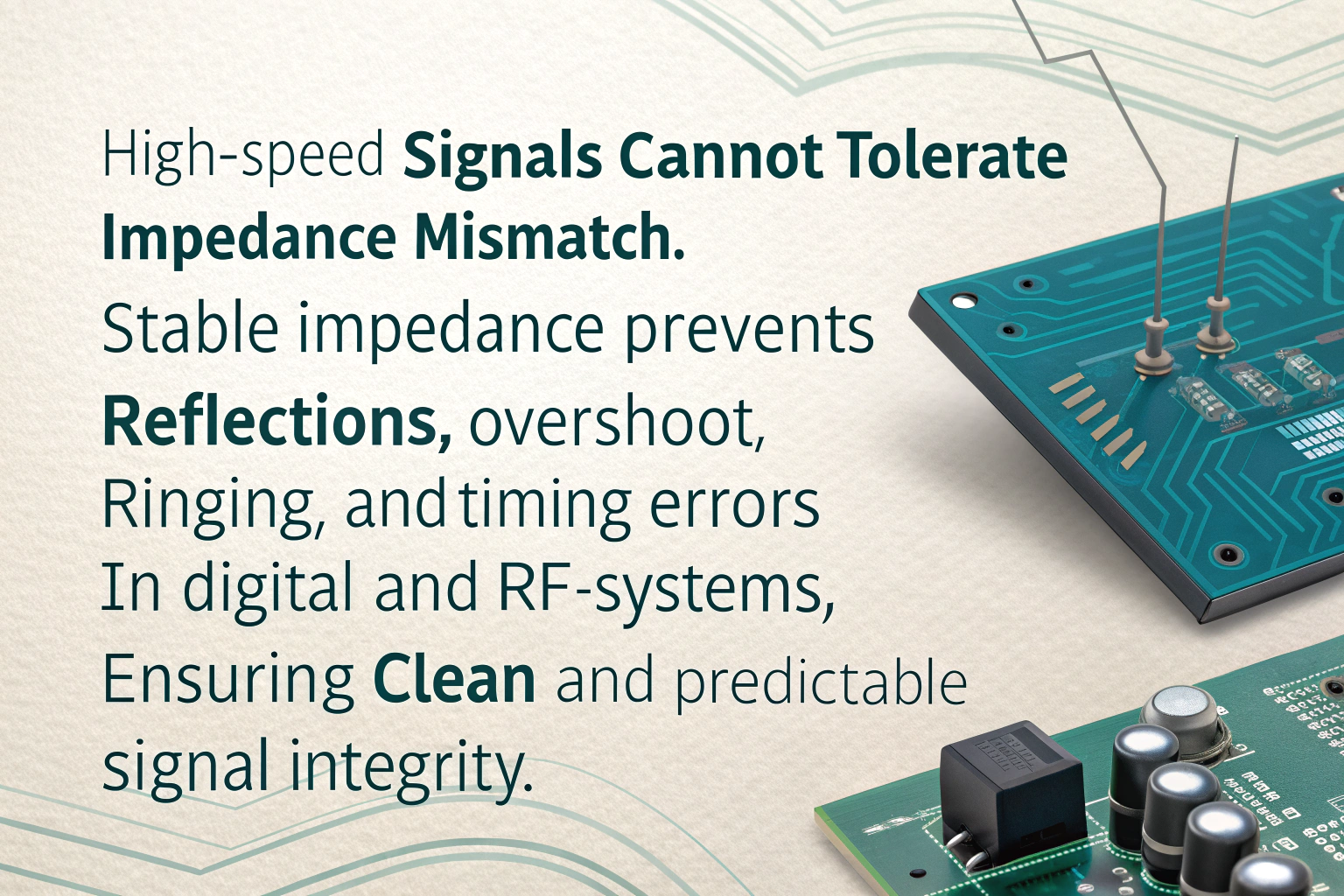
High-speed signals cannot tolerate impedance mismatch.
Stable impedance prevents reflections, overshoot, ringing, and timing errors in digital and RF systems, ensuring clean and predictable signal integrity.
Modern electronics run fast data links—USB, Ethernet, HDMI, LVDS, PCIe, and RF antennas. As edges get steeper, the PCB trace length becomes electrically significant. Without impedance control, signals bounce between mismatched points, degrading communication quality.
Detailed impact on performance
At multi-gigabit speeds, mismatches cause eye-diagram closure, packet errors, jitter accumulation, and EMI problems. Analog and RF circuits show detuning, phase shift, and unexpected noise. Differential pairs lose balance when impedance varies across layers. These issues reduce transmission margin and reliability in complex devices.
Industry considerations
Telecom, automotive, medical, and industrial control systems depend on defined signal paths for long-term stability. Manufacturers therefore perform DFM reviews, adjust stack-ups, and verify impedance coupons to guarantee compliance with high-speed interface standards.
How is controlled impedance achieved during PCB design?
Controlled impedance begins with calculation and continues through layout and stack-up definition.
Impedance is controlled by selecting the correct trace width, dielectric material, copper thickness, and PCB layer structure based on signal requirements.
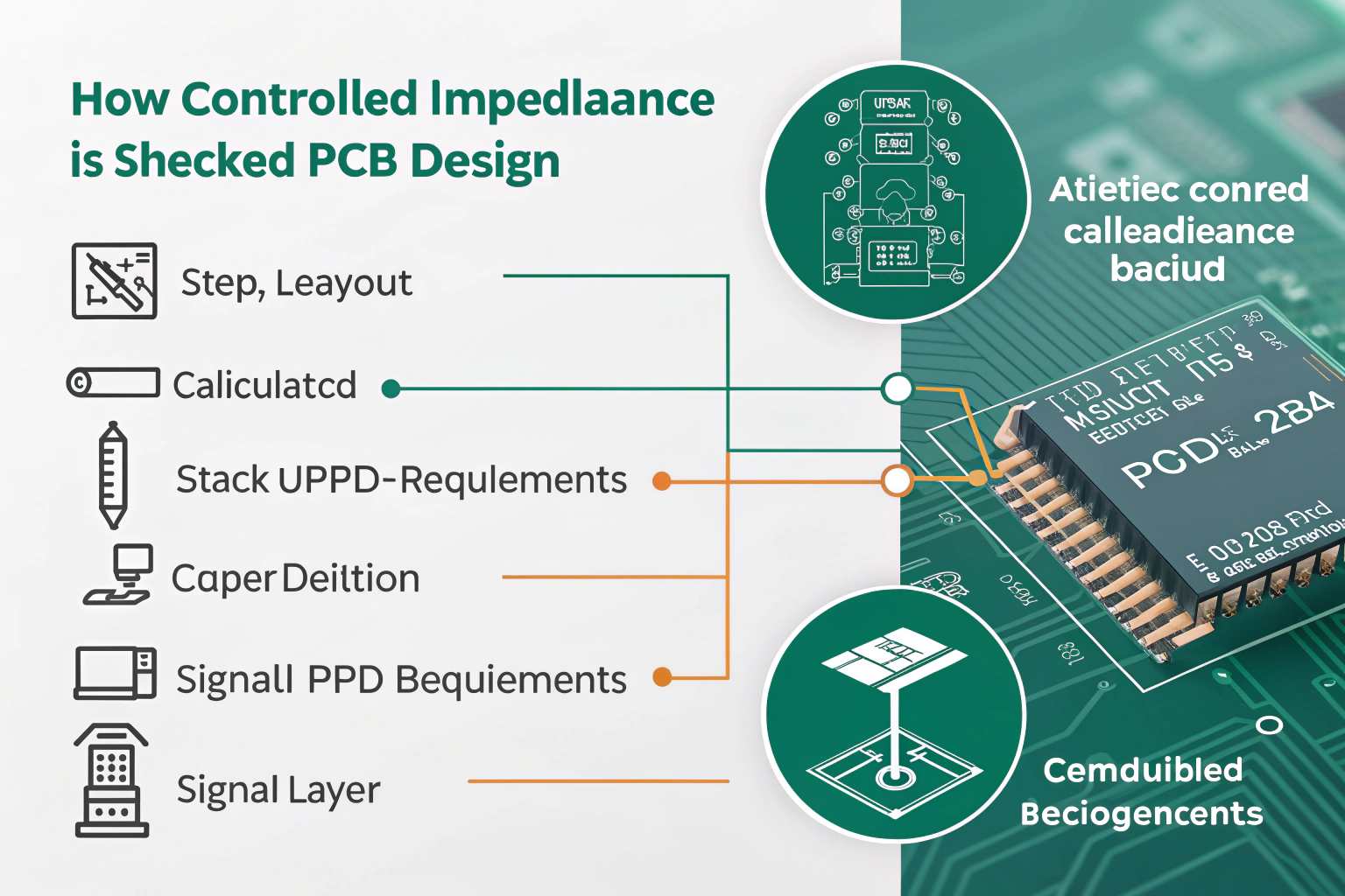
Engineers choose a target impedance based on interface specifications. Using field-solver software, the required geometry is calculated. Once finalized, the stack-up defines each layer’s dielectric thickness and material properties.
Key design factors
Trace width and spacing
Wider or narrower traces shift impedance. Differential pairs require precise spacing to maintain balance.
Dielectric thickness
Distance from the signal trace to the reference plane heavily influences impedance.
Material properties
Dielectric constant (Dk) and dissipation factor (Df) determine high-frequency behavior.
Copper thickness
Affects current distribution and therefore the characteristic impedance.
Design teams coordinate with manufacturers to confirm stack-up tolerances and ensure consistent production.
How do PCB manufacturers control and verify impedance?
Production processes must maintain tight material and dimensional tolerances.
Manufacturers control impedance through stack-up management, laminate selection, precision etching, and TDR testing of impedance coupons.
Controlled impedance requires precise processing. Any variation in dielectric thickness or copper etching changes the target value. Therefore, factories use advanced lamination controls, calibrated imaging equipment, and automated measurement systems.
Production steps for impedance control
- Maintain consistent dielectric thickness through strict lamination pressure and temperature control
- Use laser-direct imaging to form accurate trace widths
- Calibrate etching rate for uniform conductor geometry
- Perform TDR (Time Domain Reflectometry) on test coupons to verify impedance per batch
- Adjust process parameters if deviations occur
Industrial sectors requiring compliance—networking gear, automotive modules, aerospace, and fiber-optic systems—demand measured proof of impedance accuracy for every production lot.
What types of controlled impedance structures exist?
Different trace configurations support different signal requirements.
Common controlled impedance structures include microstrip, stripline, dual-stripline, coplanar waveguide, and differential pair models.
Each structure defines how the electromagnetic field propagates through or above the PCB.
Structure overview
Microstrip
A trace routed on an outer layer above a ground plane.
Stripline
A trace sandwiched between two reference planes for strong signal isolation.
Dual-stripline
Symmetrical layers providing consistent impedance for sensitive signals.
Coplanar waveguide
Controlled impedance using adjacent ground areas to confine electromagnetic fields.
Differential pairs
Two matched traces carrying equal and opposite signals for noise immunity.
These structures support high-speed digital buses, RF circuits, and precision measurement devices.
What happens when impedance is not controlled?
Uncontrolled impedance leads to instability and unpredictable performance.
Impedance mismatch causes reflections, increased EMI, data errors, detuned RF paths, and reduced overall system reliability.
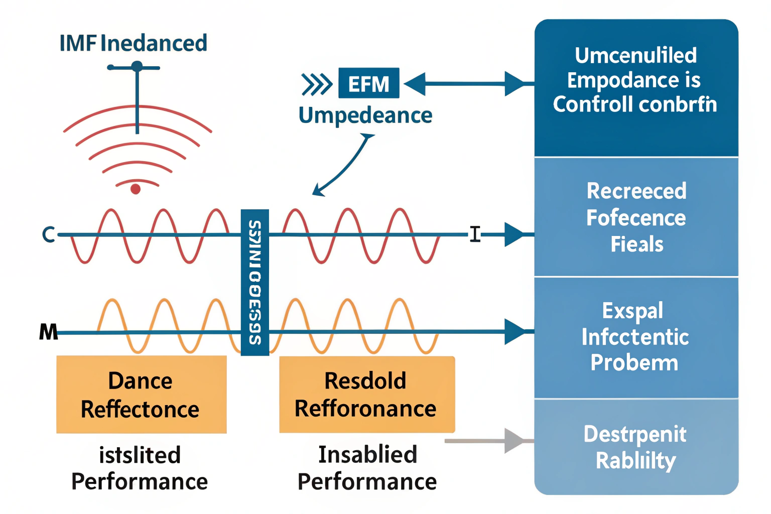
Mismatched paths distort signals as energy reflects back toward the source. This interference changes the waveform, reduces timing margin, and creates emissions that fail EMC standards.
Common issues
- Reflections that distort digital edges
- Crosstalk between adjacent traces
- Failures in Ethernet, USB, or LVDS communication
- RF detuning and reduced antenna efficiency
- Temperature-dependent instability
Long-term field reliability decreases as repeated stress accumulates on marginal links. This makes controlled impedance essential for demanding environments.
Conclusion
Controlled impedance is now a core requirement in modern PCB design and manufacturing. As data rates continue rising, signal traces behave like engineered transmission lines rather than simple copper paths. Maintaining consistent impedance ensures clean waveforms, reduced reflections, and reliable high-speed communication across every unit produced. Through accurate stack-up planning, precise geometry, proper material selection, and TDR verification, high-performance boards meet strict standards required by networking, automotive, industrial, RF, and consumer applications. With controlled impedance fully integrated into the design and manufacturing workflow, products achieve stronger signal integrity, more predictable EMC behavior, and long-lasting reliability in demanding environments. This focus on consistent electrical performance supports global competitiveness and ensures stable function in both high-speed interfaces and sensitive analog systems.
