
Yes, touching a circuit board can damage it, but the risk depends on how, where, and under what conditions contact occurs. Damage is usually not immediate or visible. Instead, it often appears later as intermittent faults, corrosion, or early failure.
Circuit boards are sensitive assemblies made of copper traces, solder joints, components, and laminate materials. Human contact introduces electrostatic discharge, moisture, oils, and mechanical stress. In manufacturing, these risks are well understood and strictly controlled.
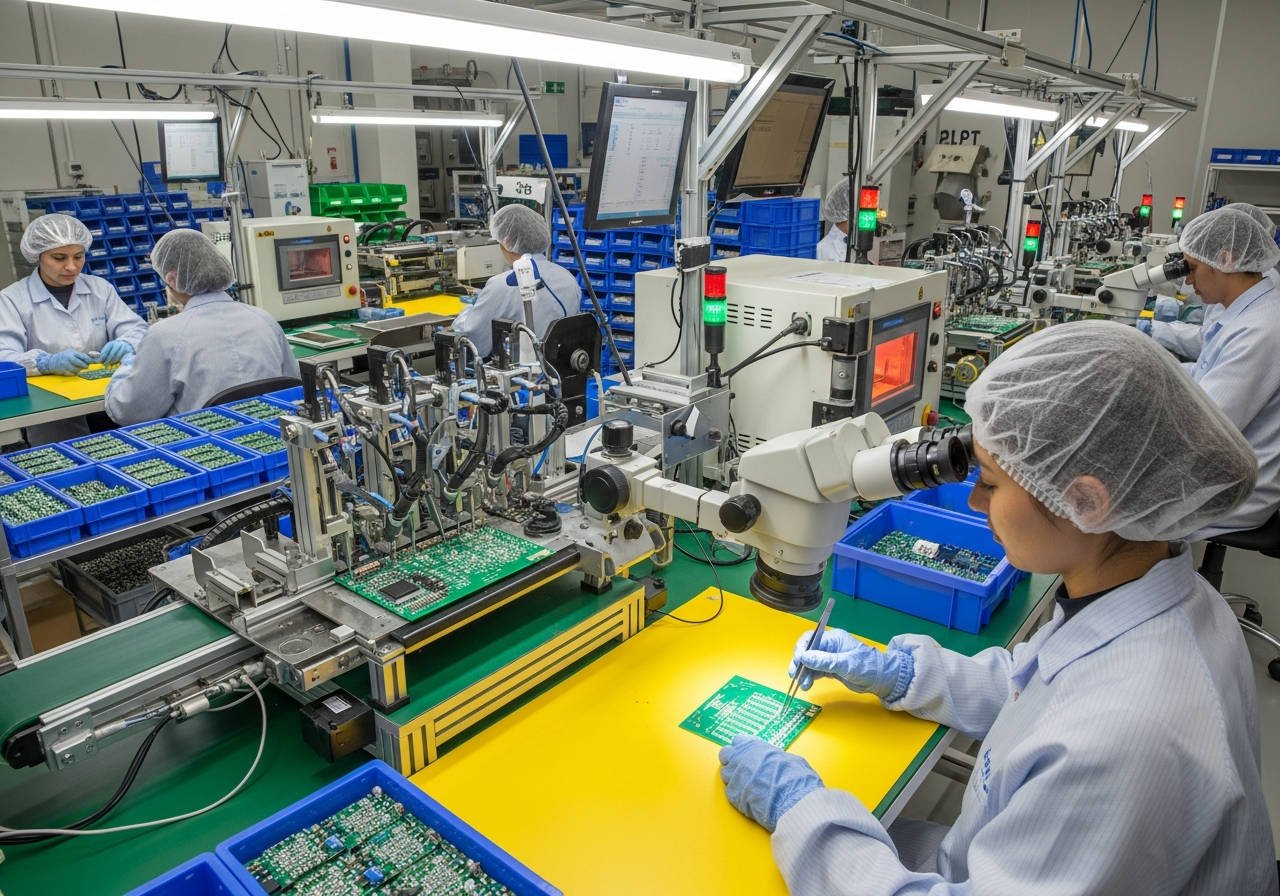
Understanding how and why touching a PCB causes damage explains why professional assembly lines treat handling as a controlled process rather than a casual action.
Why Electrostatic Discharge Is the Biggest Risk When Touching a PCB?
Electrostatic discharge is invisible but destructive.
Many failures start at the atomic level.
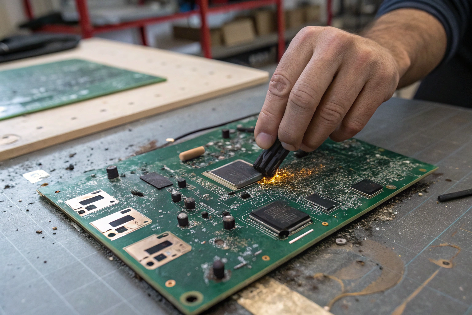
Electrostatic discharge (ESD) occurs when static electricity transfers from the human body to electronic components. Even voltages far below what can be felt by a person can damage semiconductor devices.
Sensitive components such as microcontrollers, ICs, MOSFETs, and sensors are especially vulnerable. ESD damage may not cause immediate failure. Instead, it weakens internal structures, leading to premature breakdown weeks or months later.
In factory workshops, ESD control is mandatory. This includes:
- Grounded workstations and floors
- ESD wrist straps and footwear
- Anti-static gloves and trays
- Continuous grounding monitoring
Boards are never handled directly with bare hands in controlled environments. This discipline exists because ESD damage is one of the most common hidden causes of early electronic failure.
How Skin Oils and Moisture Affect Circuit Boards?
Human skin leaves more than fingerprints.
It leaves long-term contamination.
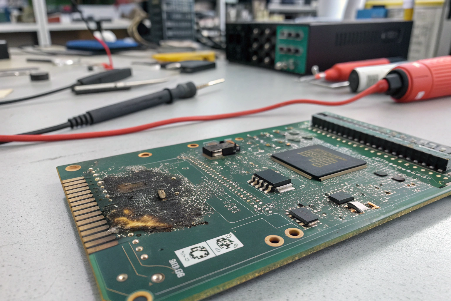
Skin oils, sweat, and salts transfer easily onto PCB surfaces. These contaminants attract moisture from the air and slowly degrade electrical insulation.
Over time, this can cause:
- Corrosion on copper traces
- Reduced insulation resistance
- Leakage currents between pads
- Poor solder joint reliability
On high-density boards, even small contamination areas can affect signal integrity. Under conformal coating or components, residues become trapped and accelerate corrosion.
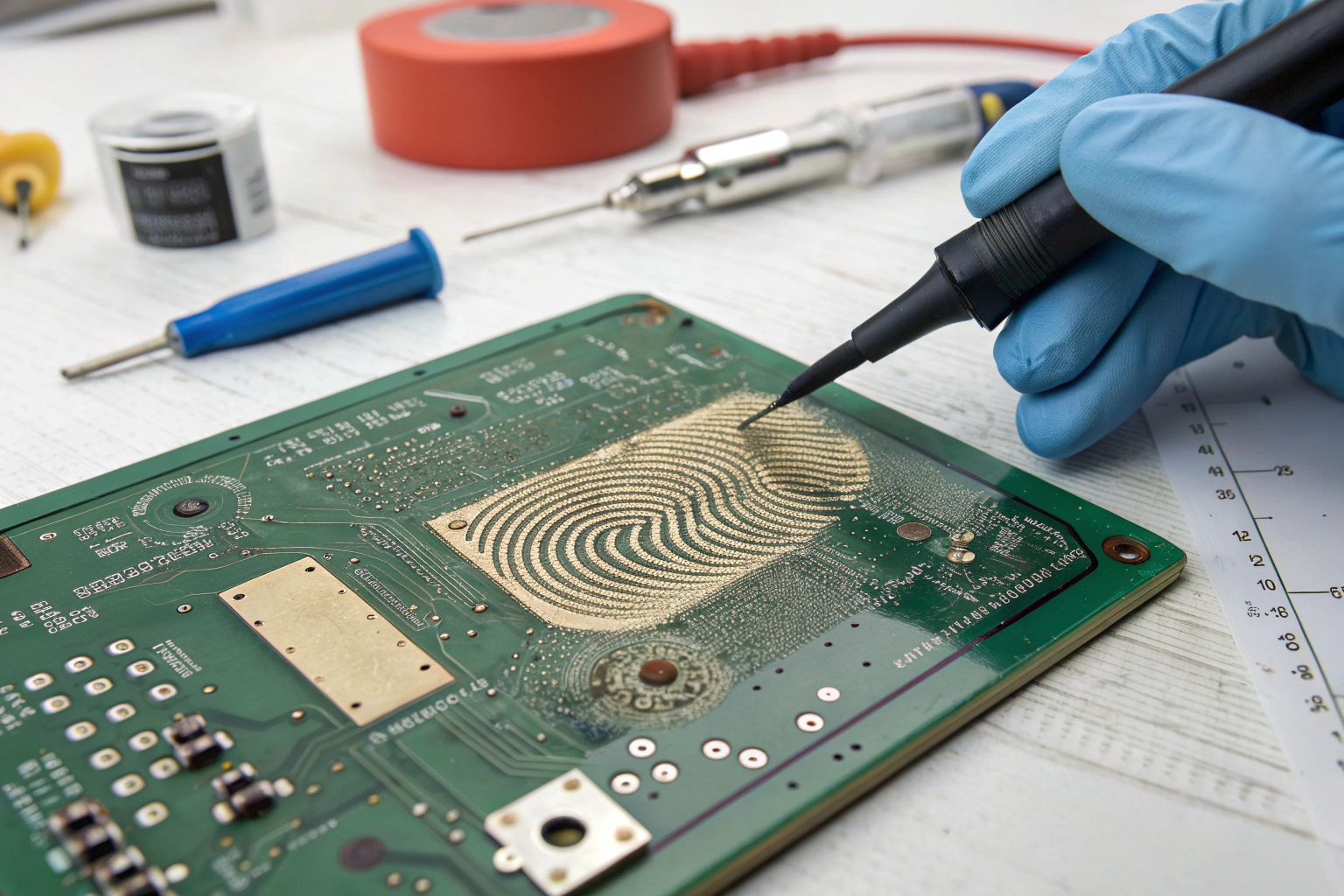
In manufacturing workshops, handling rules require gloves or finger cots. PCBs are cleaned using controlled processes after soldering to remove flux and ionic residues. Cleanliness is measured, not assumed.
Once contamination reaches internal layers or under components, it cannot be fully removed. This is why prevention is always preferred over repair.
Can Mechanical Handling Damage a PCB?
Circuit boards are rigid but not indestructible.
Stress creates hidden cracks.
Touching a PCB incorrectly often involves bending, pressing, or lifting by unsupported edges. This mechanical stress affects solder joints, vias, and internal copper layers.
Common mechanical damage includes:
- Micro-cracks in solder joints
- Cracked vias in multilayer boards
- Lifted pads near connectors
- Warping that stresses components
These defects may not appear during initial testing. They often show up later as intermittent failures when temperature changes or vibration occurs.
In factory assembly, boards are handled using fixtures, carriers, or pallets. Operators are trained to hold boards only at designated edges and support areas. Board thickness, panelization, and depaneling methods are carefully selected to minimize stress.
Mechanical damage caused by handling is one of the hardest failure modes to diagnose because it leaves little visual evidence.
Why Component Leads and Contacts Should Never Be Touched?
Not all PCB areas carry equal risk.
Contacts and leads are especially sensitive.
Touching component leads, connector pins, or exposed pads introduces contamination exactly where electrical contact is critical. Oils and salts increase contact resistance and reduce reliability.
For connectors, this leads to:
- Intermittent signal loss
- Increased heat at contact points
- Accelerated wear during mating cycles
For solderable pads, contamination reduces solder wetting and joint strength. This is a major concern during assembly and rework.
Manufacturing processes protect these areas using:
- Protective films or covers
- Controlled storage conditions
- Limited manual contact
- Incoming and outgoing inspections
Even brief contact can degrade performance in high-reliability or fine-pitch designs.
How Factory Workshops Control PCB Handling Risks?
Professional manufacturing assumes PCBs are fragile.
Processes are built to protect them.
In a controlled factory workshop, PCB handling is part of the process design. Risk is reduced through system-level controls rather than relying on individual caution.
Key handling controls include:
- ESD-protected production lines
- Defined material flow paths
- Anti-static carriers and racks
- Cleanroom or controlled environments
- Operator training and certification
Boards move through solder paste printing, placement, reflow, inspection, testing, and packaging without unnecessary manual contact. When manual handling is required, procedures define exactly how and where boards may be touched.
Environmental conditions such as humidity and temperature are monitored continuously. This prevents static buildup and moisture-related damage.
These measures ensure that touching a circuit board during production does not compromise its long-term reliability.
Is It Ever Safe to Touch a Circuit Board?
Safety depends on conditions, not intention.
Uncontrolled contact is always a risk.
In uncontrolled environments, touching a PCB with bare hands always introduces some level of risk. The absence of immediate failure does not mean no damage occurred.
In controlled environments, limited handling is allowed only when:
- ESD protection is active
- Gloves or finger cots are used
- Boards are held by edges
- Sensitive areas are avoided
Even then, handling is minimized. The goal is not to make touching safe, but to make touching unnecessary.
This philosophy reduces variation, improves yield, and extends product lifespan.
Conclusion
Touching a circuit board can damage it through electrostatic discharge, contamination, and mechanical stress. These effects are often invisible at first and appear later as intermittent faults, corrosion, or early failure. In professional manufacturing, PCB handling is treated as a critical process, supported by ESD control, cleanliness standards, mechanical protection, and trained operators. Factory workshops are designed to minimize direct contact and eliminate uncontrolled handling. Reliable electronic products are not achieved by chance. They are the result of disciplined processes that respect how sensitive circuit boards truly are. By controlling how boards are handled from assembly to packaging, long-term stability, consistency, and performance are protected throughout the entire product lifecycle.
