
Printed Circuit Boards (PCBs) are the foundational building blocks of nearly every modern electronic device—from simple calculators to complex computing systems. They serve as the physical platform that supports and connects electronic components, allowing devices to function as intended. Without PCBs, reliable and scalable electronics would not be possible.
PCBs work by channeling electrical signals through carefully engineered copper pathways. These conductive traces form intricate circuits across the board’s surface, dictating how electrical current moves between components. Each layer and connection plays a critical role in determining the performance and behavior of the finished device.
While PCB design has become increasingly digital, it remains essential for engineers—especially those new to the field—to understand the physical manufacturing process. Touring a fabrication facility and consulting with manufacturers early in the design phase can prevent costly errors. For those working with overseas suppliers, this article outlines the step-by-step PCB manufacturing process to bridge that knowledge gap and support better decision-making.
PCB Manufacturing Process Steps
Step 1: Design and Output

Every PCB begins with a meticulous design phase. Engineers use professional PCB layout software—such as Altium Designer, KiCad, OrCAD, or Eagle—to translate circuit schematics into a board layout. This layout includes copper traces, component pads, drill holes, and mechanical outlines.
Once finalized, the design is exported into a standardized manufacturing format called Gerber files (often RS-274X format). These files contain the graphical data for each layer of the PCB, including copper layers, solder masks, silkscreen, and drill data.
Before fabrication, designers should inform their manufacturer about which software version was used, to avoid potential compatibility issues. Most reputable manufacturers also perform a Design for Manufacturability (DFM) check to catch any design issues early—saving both time and cost during production.
🔗 Learn more about how Gerber files work from Altium.
Step 2: From File to Film
Once DFM validation is complete, manufacturers convert the Gerber files into photographic films using a laser photoplotter. These films serve as stencils that define each PCB layer with micrometer precision.
This process doesn’t use a typical office printer—it relies on high-resolution laser plotters capable of rendering ultra-fine circuit patterns. Each film contains a photo-negative of the corresponding PCB layer: black represents the copper traces to remain, and clear areas denote where copper will be etched away.
For two-layer boards, four films are created: two for copper layers and two for solder masks. Precise registration holes are punched in every film using an optical table system, which will ensure perfect alignment during UV exposure in the next step.
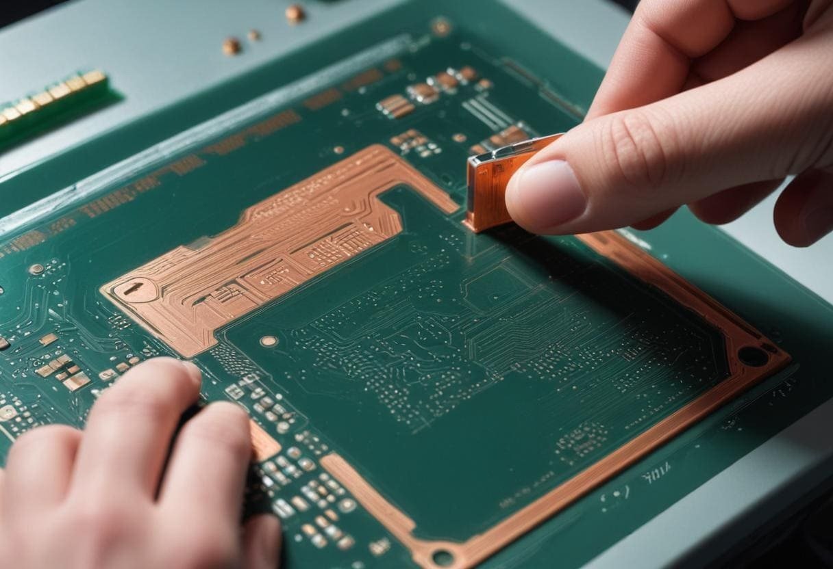
Step 3: Inner Layer Imaging – Defining Copper Routing
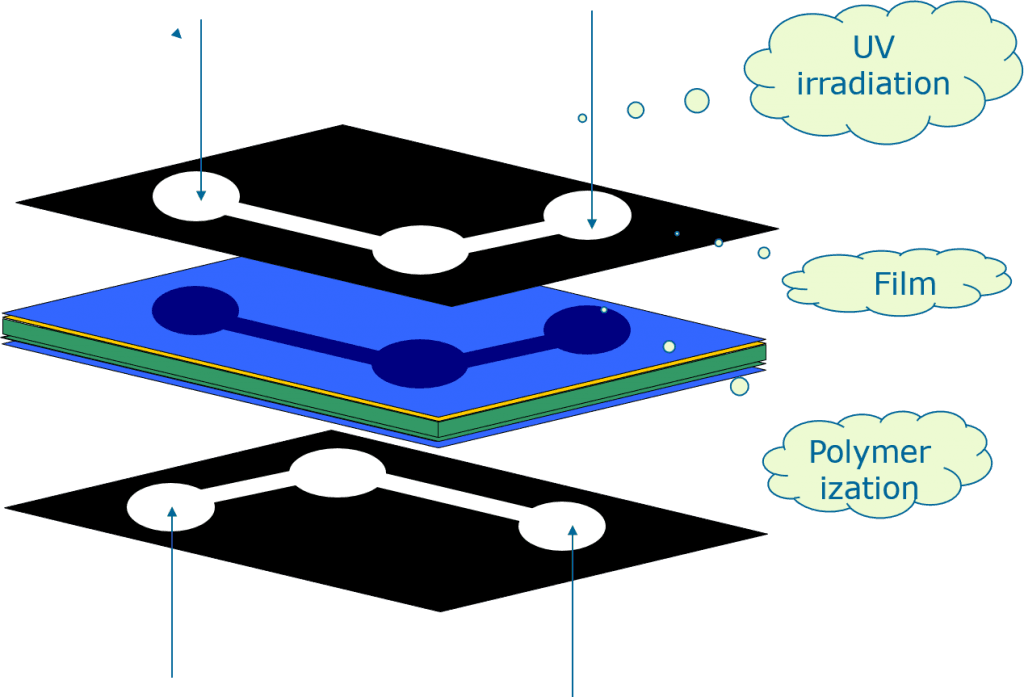
In multilayer PCBs, inner layer circuit patterns are created first. A copper-clad laminate substrate is cleaned to eliminate any oxidation or dust, which could cause electrical shorts or defects.
The board is coated with a photoresist layer—a light-sensitive polymer that reacts to UV exposure. The film from Step 2 is aligned and placed over the board using registration pins. UV light hardens the photoresist in areas where copper must remain, while dark areas on the film block the light and keep photoresist soft.
After UV exposure, the board is rinsed in a developer solution, which washes away the unhardened photoresist. This leaves behind a perfect match of the desired copper circuit pattern. A technician visually inspects the board before moving to the next process.
📘 Explore photoresist chemistry and process from BASF, a leading provider of PCB materials.
Step 4: Etching Away Unwanted Copper
Now the board contains hardened photoresist protecting only the copper you want to keep. The next step is chemical etching—where the exposed, unwanted copper is removed using a controlled acid solution (typically ammonium persulfate or ferric chloride).
This process reveals the actual copper circuit pattern that was imaged in the previous step. Once etching is complete, another solvent removes the remaining photoresist, leaving only the desired copper features.
Depending on the design, thicker copper layers may require stronger etching solutions or longer etch cycles. High-current or power PCBs typically use copper weights of 2oz or higher, demanding stricter process control.
💡 For insight on advanced etching techniques, check out this technical paper by Atotech, a global leader in PCB chemistry.
Step 5: Layer Alignment and Optical Inspection
After the inner layers are imaged and etched, they must be perfectly aligned before being laminated into a multilayer PCB. This is achieved using a high-precision optical punch system that detects the registration marks and aligns the layers based on micron-level tolerances.
Once alignment is verified, each layer undergoes automated optical inspection (AOI). This inspection uses high-resolution cameras and lasers to scan the etched patterns and compare them against the original Gerber files. If discrepancies are found, they are flagged for manual review and correction before proceeding.
Proper layer alignment is crucial—any misregistration can lead to shorts, opens, or unreliable vias in the final board.
🔍 Learn more about AOI technology in PCB fabrication from Eurocircuits.
Step 6: Layer Lamination and Bonding

Once all layers have passed inspection, they are laminated together using sheets of prepreg (pre-impregnated fiberglass with epoxy resin) and additional copper foil for the outer layers. This assembly is stacked and placed into a hydraulic lamination press that applies intense heat (typically 170–180°C) and pressure (~150–200 psi).
The heat melts the epoxy in the prepreg, which bonds the layers into a solid, unified PCB. Aluminum press plates and release films are used to ensure uniform pressure and surface smoothness during this process.
This lamination step is what transforms multiple etched layers into a single, rigid multilayer board with internal interconnections.
🛠️ For detailed lamination theory, see IPC-2222 standards on multilayer PCB design and fabrication.
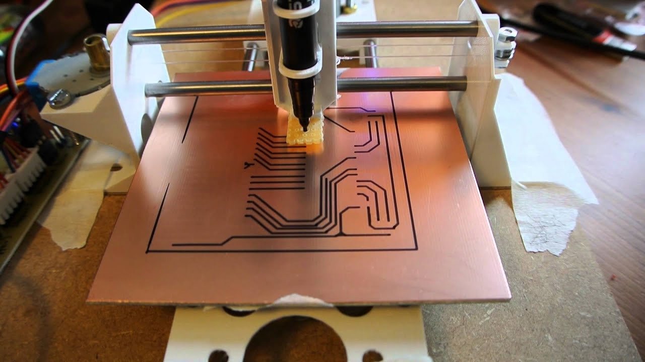
Step 7: Drilling

With the board laminated, the next step is to drill holes that will form vias and through-holes for component mounting. This is done using computer-controlled CNC drilling machines that spin at up to 150,000 RPM and can drill thousands of holes with sub-10-micron accuracy.
Before drilling, X-ray registration systems locate inner layer targets to ensure proper hole placement. Entry and exit materials are used above and below the stack to protect the board surface and avoid burrs during drilling.
These holes will later be plated with copper to create electrical connections between layers. On average, a typical 4-layer PCB might have hundreds of holes, each serving a critical purpose in the signal or power path.
Step 8: Copper Plating and Deposition
Drilled holes expose the fiberglass core, which is non-conductive. To make these holes electrically viable, the board is cleaned and then immersed in a chemical copper deposition bath.
This process—also known as electroless copper plating—applies a very thin (~1 micron) conductive copper layer across the board surface and inside the hole walls. This creates a foundation for electroplating, which later builds up the copper thickness to meet design specifications (typically 20–35 µm).
The electroless step is essential, especially for multilayer boards, because it creates conductive vias between internal copper layers. This step is fully automated and carefully controlled for pH, temperature, and metal ion concentration.
Step 9: Outer Layer Imaging
With the inner layers and plated through-holes complete, attention turns to the outer copper layers. These top and bottom layers are coated with a fresh layer of photoresist, just like in Step 3.
The panel enters a yellow room (a UV-filtered cleanroom), where it’s aligned with photo films representing the outer layer circuitry. Using pins for exact positioning, UV exposure hardens the resist in the desired copper areas.
After development, the board is inspected to verify that only the correct copper regions are exposed. This step is a mirror image of the inner layer imaging process, but with critical outer layer connections.
Step 10: Electroplating and Tin Plating
Once outer layer photoresist is patterned, the board returns to the electroplating bath. Here, the exposed copper areas are plated with a thicker layer of copper to strengthen the traces and vias. Copper is usually built up to around 25–35 µm.
Following copper plating, a thin tin layer is electroplated over the traces. This tin layer acts as an etch resist during the upcoming copper etching process, protecting the required copper features.
Precise control of plating thickness and uniformity ensures that all vias, traces, and pads meet IPC reliability standards.
Step 11: Final Etching
In this step, unwanted copper that is not protected by tin is chemically removed using an alkaline etchant. The tin remains in place, safeguarding the traces and pads during the process.
Once etching is complete, the tin layer is stripped off, leaving only the copper pathways that were defined by the photoresist and plating stages.
At this point, the PCB contains its final copper circuitry, and the outer layers now reflect the intended electrical design.
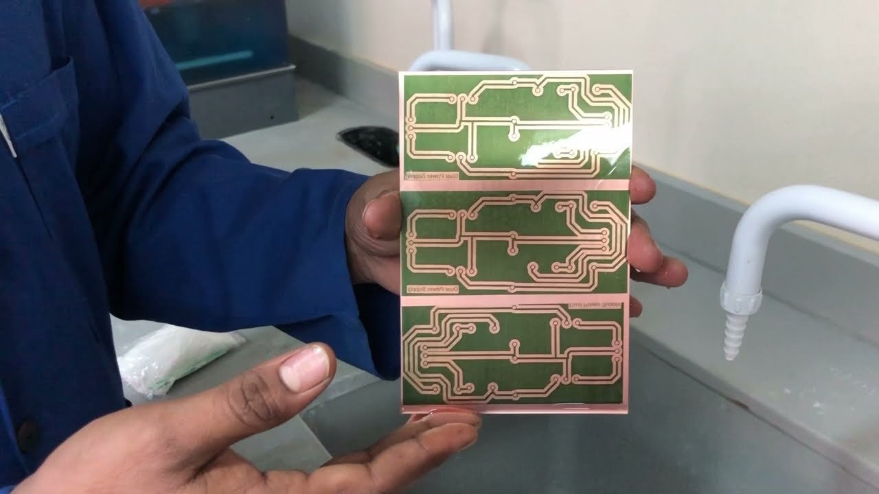
Step 12: Solder Mask Application
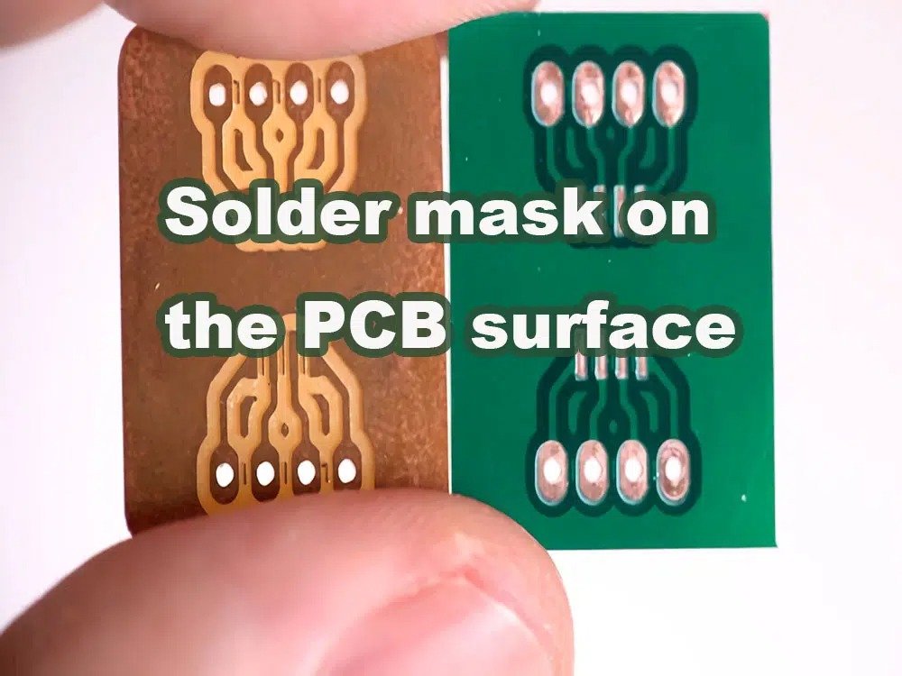
The PCB now receives a protective solder mask layer. This insulating layer prevents accidental solder bridging between closely spaced components during assembly and enhances environmental resistance.
A liquid epoxy solder mask (typically green, but other colors are available) is applied over the panel. Using UV exposure through a solder mask film, the mask is selectively hardened over all areas except for pads and exposed copper features.
The board is then baked in an oven to fully cure the solder mask, which now adds both functionality and the PCB’s characteristic appearance.
Step 13: Surface Finish
To protect exposed copper and ensure solderability, the PCB receives a surface finish. This coating enhances the bond between the PCB and the solder during assembly.
Common surface finishes include:
- HASL (Hot Air Solder Leveling) – economical and widely used
- ENIG (Electroless Nickel Immersion Gold) – excellent for fine-pitch components
- OSP (Organic Solderability Preservatives) – lead-free, cost-efficient
- Immersion Silver or Tin – for high-speed signals or RoHS compliance
Each finish has specific advantages based on board type, environment, and assembly method.
🔗 For a full comparison, check Eurocircuits’ surface finish guide.
Step 14: Silkscreen Application
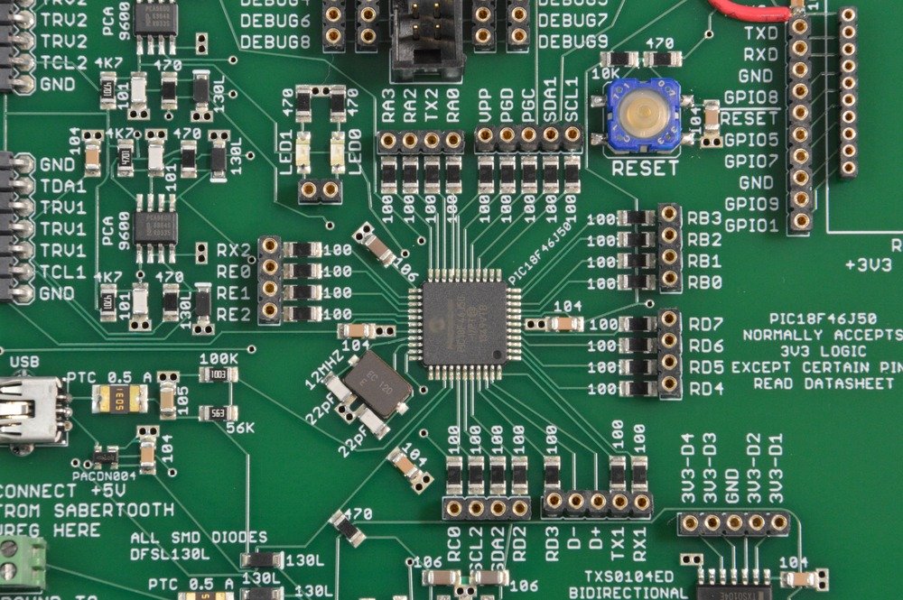
The silkscreen layer is applied to print text and graphics onto the PCB. This includes component labels, test point IDs, company logos, date codes, and any important assembly markings.
Modern PCB fabrication uses automated inkjet or screen-printing technology, followed by UV or thermal curing, to apply white or black ink depending on solder mask color.
Clear, well-aligned silkscreen enhances assembly accuracy and serviceability.
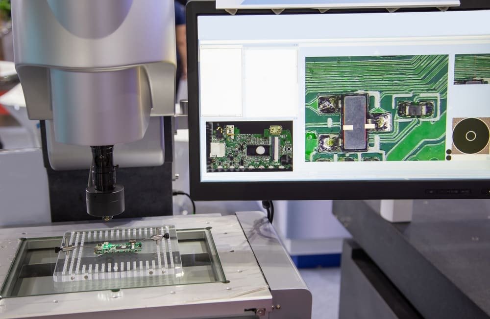
Step 15: Electrical Testing
Before delivery, every board undergoes electrical testing to verify continuity, isolation, and net integrity. There are two primary methods:
- Flying Probe Testing – used for low- to mid-volume and prototypes
- Bed-of-Nails (fixture) Testing – used for high-volume production
These systems compare the actual connectivity of the fabricated PCB with the original netlist generated from the design files. Failures are flagged and logged for further analysis.
📐 More on flying probe testing vs. bed-of-nails from Cadence Design Systems.
Step 16: Profiling and V-Scoring
The final step is to separate individual PCBs from the manufacturing panel. Two main methods are used:
- CNC Routing – leaves breakaway tabs, useful for custom shapes
- V-Scoring – partial-depth cuts along panel lines for easy snap-off
Boards are then cleaned, packaged in anti-static vacuum-sealed bags, and labeled for shipment.
High-quality manufacturers also include moisture indicator cards, desiccant, and lot tracking for traceability.
Conclusion
From concept to production, PCB manufacturing is a tightly controlled, precision-driven process that transforms digital designs into robust physical hardware.
Each step—design, imaging, drilling, plating, masking, and testing—is critical in ensuring long-term performance, reliability, and safety of electronic products.
Whether you’re working on prototypes or volume production, partnering with a manufacturer that offers end-to-end process control, real-time DFM feedback, and certified QA systems (like ISO 9001 and IPC-A-600) can drastically improve time to market and final product quality.
📌 Want help with your next PCB project?
Check out CustomPCBA — a trusted full-service PCB fabrication and assembly partner offering quickturn prototypes, scalable volume production, and full testing services.
