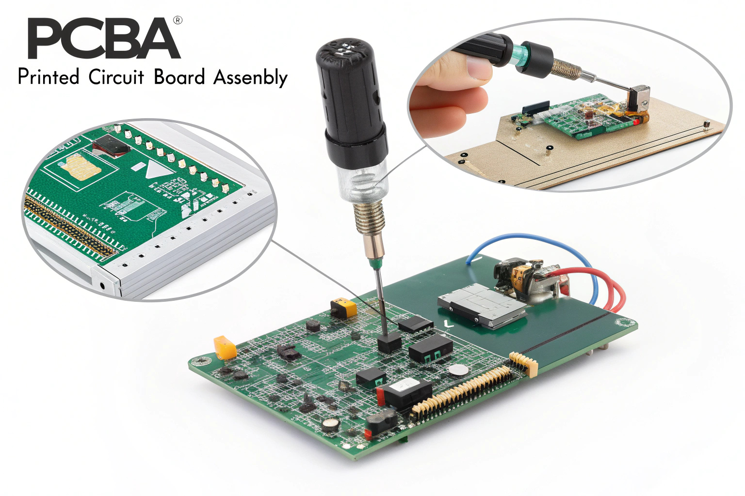
CBAA is the foundation of every functioning electronic device—but what exactly happens during the PCBA assembly process?
The PCBA (Printed Circuit Board Assembly) process involves mounting and soldering electronic components onto a blank circuit board, transforming it into a fully functional module.
Electronics have become inseparable from our daily lives. From mobile phones to smart TVs and industrial automation, everything runs on complex yet compact electronic circuits. But none of that is possible without PCBAA, or Printed Circuit Board Assembly and Automation. This process turns a passive circuit board into an active brain of a device by integrating all essential electronic components.
If you’ve ever been curious about what happens between designing a PCB and seeing it power your device, this guide offers a clear breakdown of how PCBA works—from paste application to final inspection.
✔
PCBAA refers to the process of mounting and soldering components onto a printed circuit board—distinct from the bare PCB itself.
✖
Modern PCBAA relies heavily on automation. Machines handle most soldering tasks for improved speed, accuracy, and consistency.
What Is PCBAA?

PCBAA stands for Printed Circuit Board Assembly and Automation. It describes the full process of taking a bare PCB and turning it into a working electronic system by mounting and soldering components such as resistors, capacitors, diodes, and microcontrollers.
The distinction between PCB and PCBAA is important. A PCB is the flat board with copper traces; a PCBA is that same board after components are added. The extra "A" in PCBAA refers to the modern automation technologies used in high-speed production lines, where machines handle nearly every step of the process.
In high-volume manufacturing, PCBAA ensures precision, scalability, and reliability. Even the tiniest smartphone circuit passes through dozens of robotic steps to ensure performance and consistency.
Step-by-Step Overview of the PCBA Assembly Process
The PCBAA process typically follows these stages:
Solder Paste Application – A stencil is used to apply solder paste to the board’s pads.
Component Placement – High-speed machines place tiny electronic parts with micrometer accuracy.
Reflow Soldering – The board is passed through an oven that melts the solder paste to bond components.
Through-Hole Component Insertion – For larger or legacy parts, leads are inserted into drilled holes.
Wave Soldering (if THT) – Boards with through-hole parts are soldered by passing over a wave of molten solder.
Inspection and Testing – Optical and functional tests check for solder defects, missing parts, and electrical failures.
Each of these stages must be executed with precision to ensure the final product functions reliably under real-world conditions.
For a visual breakdown of this process, see this PCBA guide from Tempo Automation.
SMT vs THT in PCBAA

The PCBAA process mainly uses two component mounting techniques: Surface Mount Technology (SMT) and Through-Hole Technology (THT).
SMT components are smaller, mounted directly onto the surface of the PCB, and used in most modern devices. Their small size allows for compact, multi-layer boards and high-speed manufacturing.
THT components have leads that go through holes in the PCB. While less space-efficient, they provide strong mechanical bonds and are preferred in applications that require durability—like automotive or aerospace electronics.
Today’s PCBAA often uses a hybrid of both, depending on the product’s design and intended use.
Testing and Quality Control
Quality assurance is critical in PCBAA, especially when even a single faulty board can lead to device failure. Manufacturers use a range of inspection methods:
- Automated Optical Inspection (AOI) checks for misplaced or missing parts.
- X-ray inspection examines solder joints hidden beneath BGAs (Ball Grid Arrays).
- Functional Testing (FCT) simulates how the board performs under real usage.
These inspections ensure the final product meets industry standards and performs reliably. According to Sierra Circuits, thorough testing can reduce field failure rates by up to 80%.
Common PCBAA Challenges
Despite automation, PCBAA still faces common challenges:
- Solder Bridging: Excess solder connecting adjacent pins.
- Tombstoning: Components standing up due to uneven solder melting.
- Component Misalignment: From vibration or improper stencil application.
- Electrostatic Damage: Sensitive parts affected by static electricity during assembly.
Preventing these issues requires well-calibrated machines, proper environment controls, and experienced process engineers.
Conclusion
The PCBAA process is the unseen hero of modern electronics. It transforms passive copper-lined boards into intelligent systems capable of processing data, powering screens, and communicating wirelessly. Through a combination of automated precision and rigorous testing, PCBAA enables today’s technology to be compact, reliable, and scalable.
As electronics continue to shrink while increasing in power, PCBAA will remain at the core of innovation—connecting the design vision to real-world performance. Whether you’re a product developer or just tech-curious, understanding how PCBAA works brings you one step closer to how our digital world operates behind the scenes.

