
Printed Circuit Boards (PCBs) and Printed Circuit Board Assemblies (PCBAs) are foundational to the electronics industry, yet they represent distinctly different stages in the product lifecycle. While a PCB refers to the bare circuit board, a PCBA represents the fully assembled, functional board equipped with all necessary components. Understanding the difference between the two is essential for engineers, procurement teams, and OEMs looking to bring electronic designs to life.
What Is a Printed Circuit Board? (PCB)
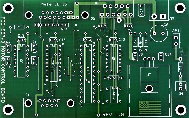
A Printed Circuit Board (PCB) is the fundamental substrate that supports and connects electronic components within a device. It typically consists of a non-conductive base material—such as FR-4 fiberglass epoxy—laminated with one or more layers of copper foil. These copper layers are etched into intricate patterns that form the board’s electrical circuitry.
PCBs may be single-layered or multi-layered, depending on the complexity of the electronic design. Each layer serves specific electrical and mechanical functions, such as routing signals, distributing power, and shielding against electromagnetic interference. Although a PCB is inert in its unassembled form, it provides the structural and electrical foundation upon which the rest of the device is built.
What Is a Printed Circuit Board Assembly? (PCBA)
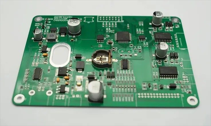
A Printed Circuit Board Assembly (PCBA) refers to the completed product that results after electronic components are mounted onto a bare PCB. This process transforms the passive circuit board into an active, functional unit capable of performing the designed electrical tasks.
The PCBA process includes several key steps:
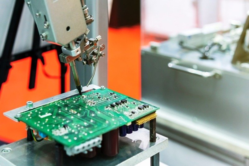
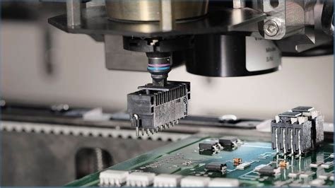
- Surface Mount Technology (SMT) or Plated Through-Hole (PTH) assembly
- Component placement via automated pick-and-place systems
- Soldering (typically reflow or wave soldering)
- Quality control using optical inspection, X-ray, and functional tests
PCBA is not just a manufacturing step—it is where design becomes real. Every trace, via, and solder joint must perform perfectly to ensure reliable device operation. At custompcba, we provide full turnkey assembly services, ensuring accuracy, repeatability, and compliance with global standards.
What Are the Different Types of PCBs?
PCBs are available in various configurations to meet diverse design and performance requirements. Here are the most common types:
Single-Layer PCBs
These boards contain a single conductive layer on one side of the substrate. They are simple and inexpensive, suitable for low-density applications such as LED panels, power supplies, and basic consumer gadgets.
Double-Layer PCBs
Featuring copper layers on both sides of the board, double-layer PCBs allow for more complex routing and greater component density. Connections between the two sides are made using plated through-holes (vias).
Multi-Layer PCBs
These consist of three or more conductive layers stacked with insulating material in between. Multi-layer PCBs are used in sophisticated electronics such as computers, telecom systems, and medical imaging devices, where space efficiency and high signal integrity are essential.
Flexible and Rigid-Flex PCBs
- Flexible PCBs use polyimide film and can bend to fit compact enclosures.
- Rigid-Flex PCBs combine rigid and flexible layers, enabling 3D configurations often required in aerospace, defense, and wearable tech.
What Are the Most Common Assembly Methods for PCBs?
The method used to assemble a PCB depends on component type, performance demands, and manufacturing strategy.
Surface Mount Technology (SMT)
SMT involves placing small, leadless components directly onto the board’s surface. Solder paste is first applied to the pads, then components are placed by machines, and finally passed through a reflow oven to solidify the connections.
Advantages:
- High component density
- Faster assembly and automation-friendly
- Ideal for multi-layer boards and compact designs
Through-Hole Technology (THT)
In THT, components with long leads are inserted into drilled holes on the PCB and soldered from the opposite side. It’s more labor-intensive but offers stronger mechanical bonds.
Advantages:
- Greater mechanical stability
- Preferred for power components and connectors
- Easier for prototyping and manual rework
Mixed Technology
Many designs combine SMT and THT, especially when high-current connectors or transformers are required. Mixed assemblies leverage the benefits of both approaches to meet complex performance and durability standards.
What Kind of Materials Are Used for Printed Circuit Boards?
Material selection impacts a PCB’s thermal performance, electrical reliability, and environmental durability.
Substrate Materials
- FR-4: Industry standard, flame-retardant fiberglass epoxy
- Polyimide: Heat-resistant, used in flexible circuits
- Metal-core PCB (MCPCB): Used in high-heat applications like LED lighting
Conductive Layers
- Copper is the primary material for traces, usually between 1oz and 3oz per square foot
- High-current applications may use thicker copper layers up to 6oz
Surface Finishes
- HASL (Hot Air Solder Leveling): Common and cost-effective
- ENIG (Electroless Nickel Immersion Gold): Superior flatness and solderability
- Immersion Silver/Tin: Used for specific signal or environmental needs
At custompcba, we help clients choose the optimal combination of base materials, copper weight, and surface finish based on current requirements, signal frequency, and reliability expectations.
What Are the Applications for PCBs?
PCBs are ubiquitous across nearly every modern industry. Their compactness, durability, and design flexibility make them ideal for applications ranging from consumer electronics to mission-critical aerospace systems.
Examples of common PCB applications:
- Consumer: Smartphones, TVs, game consoles, wearable devices
- Automotive: Engine control units, infotainment, ADAS systems
- Medical: Imaging equipment, pacemakers, diagnostics
- Industrial: Automation, robotics, PLCs, motor controllers
- Telecom: Base stations, networking switches, satellites
- Aerospace: Navigation, control panels, avionics systems
Each application imposes its own set of requirements—signal speed, thermal dissipation, reliability—which custompcba accounts for during both PCB design and PCBA stages.
What Is the Cost of PCBAs?
Several variables affect the final cost of a PCBA:
Key Pricing Factors:
- Component pricing: ICs, passives, connectors
- Labor: Manual assembly vs automation
- Tooling & setup fees: For stencils, fixtures, or non-standard board shapes
- Volume: Higher order quantities reduce per-unit cost
- Turnaround time: Expedited orders carry surcharges
- Technology type: SMT is typically less labor-intensive than THT
- Testing & inspection requirements
- Packaging & shipping
Additionally, geographical location plays a significant role. While some offshore assembly houses offer low prices, it often comes with trade-offs in communication, lead time, and quality. At custompcba, we offer globally competitive pricing without compromising technical performance or support.
How to Pick a PCBA Manufacturer?
Choosing the right assembly partner can determine the success—or failure—of your product.
What You Should Look For:
- Capacity: Can the manufacturer scale with your production needs?
- Certifications: ISO 9001, IPC-A-610, RoHS compliance
- Engineering support: DFM (Design for Manufacturability) reviews and prototyping services
- Testing capabilities: AOI, ICT, functional testing, X-ray inspection
- Clear pricing structure: Transparent quotes with no hidden fees
- Track record: Experience in your industry or product category
Most importantly, your PCBA partner should act as a true collaborator—not just a supplier. At custompcba, we integrate with your design team early, prevent downstream errors, and ensure that every board shipped meets rigorous quality standards.
Conclusion
While PCB and PCBA are closely linked, they represent different stages in a product’s lifecycle. The PCB is a bare, passive platform; the PCBA is the fully functional result of careful assembly, inspection, and testing.
Understanding their roles helps you make better decisions about design, production, and partnerships. Whether you’re developing a prototype or launching mass production, working with a trusted partner like custompcba ensures quality, scalability, and long-term product success.
