
SMT assembly vs through-hole technology is a key consideration when designing or manufacturing a PCB. But what do these two methods mean, how do they differ, and when should you choose one over the other?
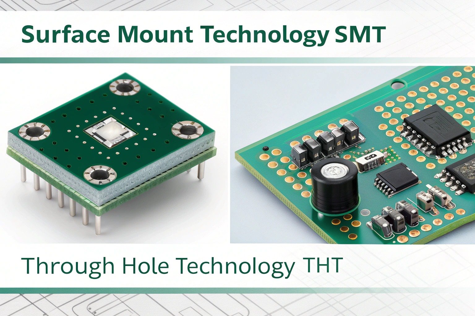
Surface Mount Technology (SMT) and Through-Hole Technology are two essential PCB assembly methods. SMT involves placing components directly onto the board’s surface, while Through-Hole requires inserting component leads through drilled holes.
Whether you’re designing a modern wearable or a rugged industrial control board, understanding the difference between SMT and Through-Hole will help you make better design, cost, and reliability decisions. This guide breaks down both methods and explains when and why each one is used in electronics manufacturing today.
What Is SMT Assembly?
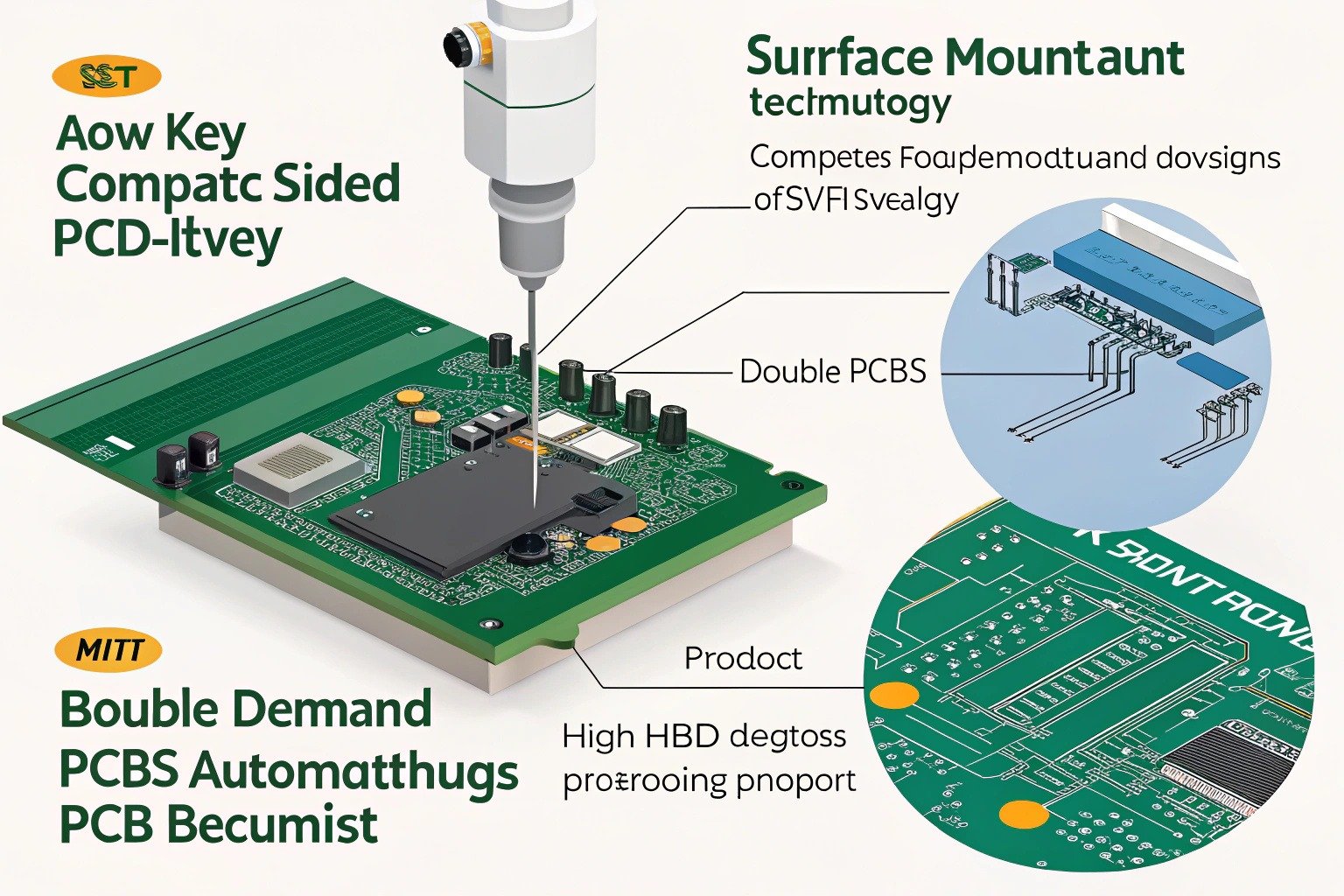
SMT (Surface Mount Technology) is a widely adopted PCB assembly technique in which components are placed directly onto the surface of the printed circuit board. Unlike traditional methods, SMT doesn’t require drilling holes for component leads, which streamlines the manufacturing process.
This method is especially favored for:
- Compact and lightweight device designs
- High-density, double-sided PCBs
- Automated mass production with high throughput
Thanks to automated pick-and-place machines, SMT supports high-speed assembly and precise component placement. SMT components, also known as SMDs (Surface Mount Devices), are typically smaller, lighter, and more efficient for modern applications like smartphones, wearables, and IoT modules.
For more on how SMT lines work, explore this intro from JLCPCB, one of the most popular PCB manufacturers globally.
What Is Through-Hole Technology?
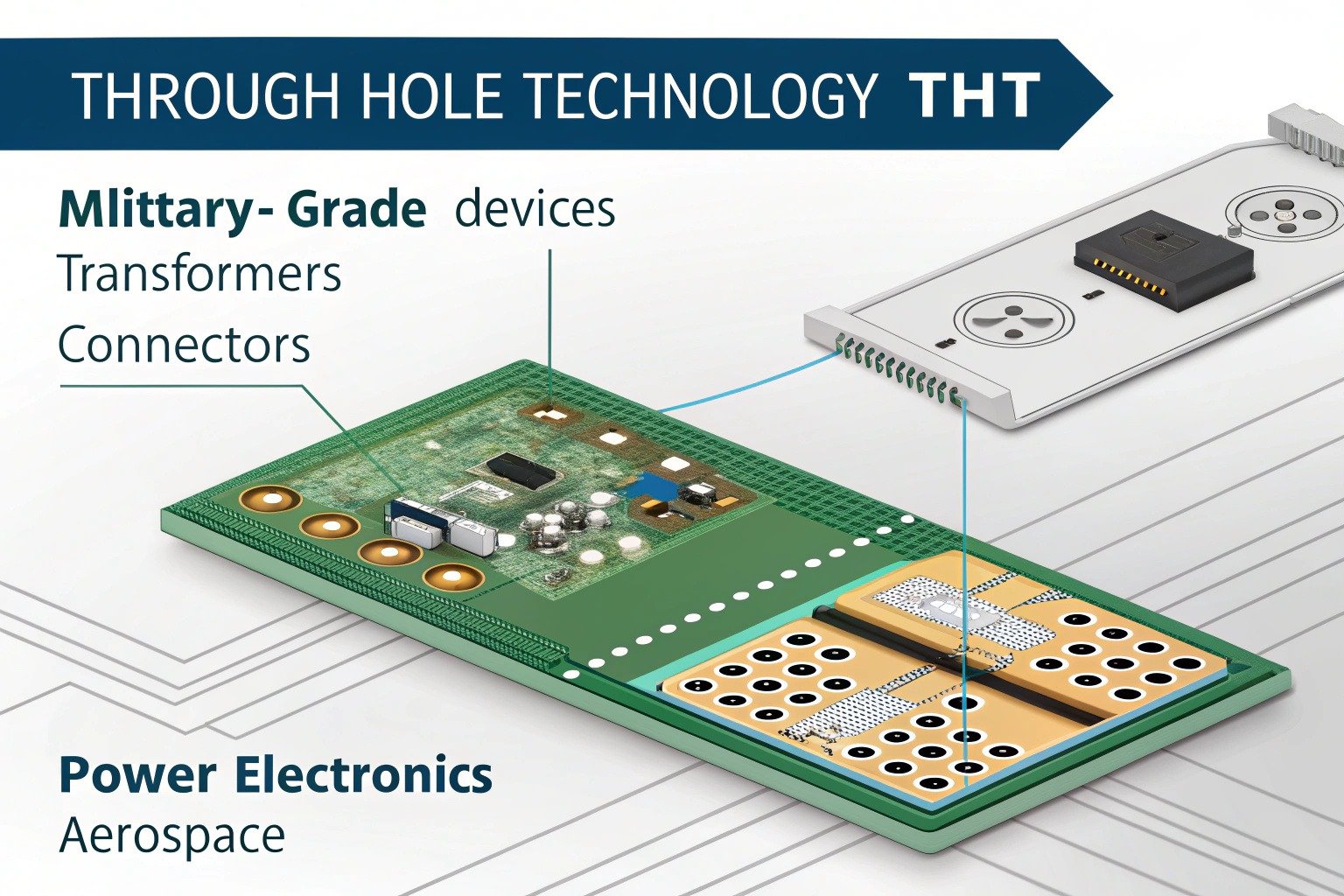
Through-Hole Technology (THT) refers to the older, but still essential method of inserting component leads through pre-drilled holes on a PCB. These leads are soldered on the opposite side, providing a strong mechanical and electrical connection.
Though slower and more labor-intensive, Through-Hole is still used in:
- Power electronics
- Aerospace and military-grade devices
- Large components like transformers, relays, or connectors
- Environments with high vibration or thermal stress
This method is typically used where physical durability and manual assembly or prototyping are required. The robustness of through-hole joints also makes them more reliable for mission-critical applications.
Core Differences Between SMT and Through-Hole
Although both methods are essential in the world of PCB assembly, they serve different needs and suit different applications.
Here’s a side-by-side comparison:
| Feature | Surface Mount (SMT) | Through-Hole (THT) |
|---|---|---|
| Assembly Method | Mounted directly on PCB surface | Inserted through holes and soldered |
| Component Size | Small, low-profile | Larger, with long leads |
| Automation | Highly automated process | Often manual or semi-automated |
| Mechanical Strength | Moderate | High (ideal for stress-heavy components) |
| Production Volume | Best for high-volume manufacturing | Ideal for low to medium volume or prototyping |
| Double-sided PCB | Easily supported | More complex and costlier |
| Ideal Applications | Mobile devices, consumer electronics | Industrial controls, aerospace, power boards |
✅ Pro Tip: Most modern boards use a hybrid assembly strategy—SMT for most components, and THT for parts that require additional strength or current-handling capacity.
When to Choose SMT vs. Through-Hole
Choosing between SMT and Through-Hole assembly depends on your product’s goals, environment, and scale.
If your priority is compact design, fast production, and automated assembly, SMT is the clear winner. It minimizes board space, reduces material costs, and speeds up the entire manufacturing line. SMT is the go-to method for smartphones, tablets, cameras, and smart appliances.
However, if your device requires mechanical resilience, frequent component swapping, or must endure thermal cycling or vibration, Through-Hole is still relevant. For example, PCBs in heavy machinery or aerospace avionics often use THT for critical connectors or relays that must never fail.
Many contract manufacturers, like MacroFab, specialize in helping teams combine SMT and Through-Hole intelligently, allowing your product to get the best of both worlds.
Conclusion
Understanding the strengths of Surface Mount Technology vs. Through-Hole Assembly is essential for anyone involved in product development or PCB design. These two technologies aren’t competitors—they’re tools, and the key is knowing when to use which.
SMT offers efficiency, density, and scalability. Through-Hole provides strength, reliability, and repairability. Most modern electronic products leverage both methods in a single design to balance speed, cost, and durability.
Next time you’re preparing a BOM or working on a layout, ask yourself: what kind of assembly does this board really need? The right decision here can save you time, money—and deliver a better product to your users.
