
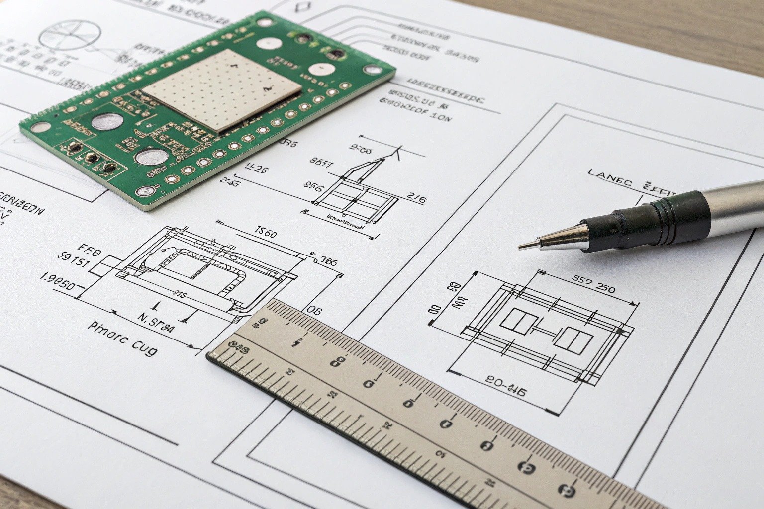
A PCB fab drawing (short for PCB fabrication drawing) is an essential document used during PCB manufacturing. It provides critical production data such as board dimensions, drill hole locations, layer stack-up, material specifications, and tolerances. If you’re wondering what should a PCB fab drawing include, this guide will walk you through every key element to help ensure your design is correctly manufactured.
The PCB fab drawing provides essential manufacturing instructions, including the layer configuration, hole plating, component placements, mechanical outlines, and other physical specifications. Manufacturers rely on it to build the PCB according to the design requirements.
Creating a PCB involves multiple stages, from electrical design to physical production. While design files define the circuit, the PCB fab drawing details how the board should be fabricated, making it a critical part of the documentation package. In this article, we’ll explore exactly what a comprehensive PCB fab drawing should include to ensure a smooth transition from design to fabrication.
What is a PCB Fab Drawing?
A PCB fab drawing is a technical document provided to the PCB manufacturer that outlines all the necessary details about the board’s physical and mechanical features. It acts as a guide for fabricating the board, complementing the design files (Gerber files) by providing additional data such as layer information, drilling instructions, material choices, and tolerances.
PCB fab drawings are particularly important for multi-layer, complex designs where precise measurements, material types, and layer configurations must be clearly specified. For simpler designs, they still provide valuable documentation to avoid mistakes during production.
Key Elements of a PCB Fab Drawing
Layer Stack-Up
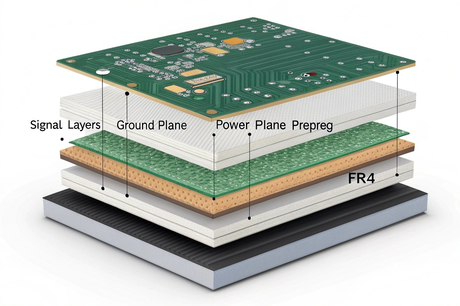
The layer stack-up is a critical part of the fab drawing. It specifies how the PCB’s layers will be arranged, including the number of signal, power, ground, and other layers (e.g., copper layers). The stack-up also includes the thickness of each layer and the material used for each layer, such as FR4 or other specialized materials.
The layer stack-up ensures that the manufacturer understands the correct order of layers and the required thicknesses for each, which directly impacts the electrical and mechanical properties of the final product.
Drill Drawing
A drill drawing is another essential part of the fab drawing. It includes precise information about the location, size, and type of holes or vias that need to be drilled into the PCB. This includes through-holes, blind vias, and buried vias.
The drill drawing must also specify the tolerances for hole sizes, as slight deviations can affect component placement and the electrical performance of the board. This is crucial for ensuring that all components are properly placed and that electrical signals can flow correctly through the PCB.
Solder Mask and Silk Screen Layers
The solder mask layer defines the areas of the PCB that will be covered by a layer of protective coating, leaving the pads exposed for component soldering. The solder mask is essential for preventing solder bridging and improving the reliability of the board.
The silk screen layer is used to print identifying marks on the PCB, such as component designators, logos, and other helpful labels. This layer is essential for both assembly and debugging, providing clear identification of components and connections.
Component Placement and Pad Design
The component placement and pad design section in the fab drawing specifies the exact locations for each component, along with the dimensions of the pads. This is crucial for ensuring that components are correctly positioned during assembly, reducing the risk of misalignment or placement errors.
Additionally, pad design is particularly important to match the size and shape of the component leads with the solder pads, ensuring proper soldering and electrical contact.
Material Specifications
Material choices are a crucial aspect of the fab drawing. The drawing should specify the type of PCB material (such as FR4, Rogers, or flexible substrates) and the desired properties, including dielectric constant, heat resistance, and copper thickness.
These materials significantly impact the electrical performance and durability of the final PCB, especially in high-speed, high-frequency, or high-power applications.
Mechanical Dimensions and Tolerances
The mechanical dimensions section outlines the overall size of the PCB and any special dimensions required, such as cutouts, notches, or holes for mounting. It also specifies the tolerances for these dimensions to ensure that the manufacturer can produce the PCB with the necessary precision.
Correct mechanical dimensions ensure that the board fits properly into its intended enclosure or system and that components align with external interfaces.
Why Is a PCB Fab Drawing Important?

A well-prepared PCB fab drawing is crucial for ensuring the board is fabricated according to the designer’s specifications and can be assembled without issues. It helps prevent mistakes that could lead to costly production delays or failures in the final product. Some key reasons why fab drawings are essential:
- Manufacturing Accuracy: It ensures that all specifications, such as layer stack-up, material types, and drill sizes, are communicated clearly to the manufacturer.
- Improved Communication: Fab drawings provide a clear, visual representation of the design, reducing the risk of miscommunication between the designer and the manufacturer.
- Consistency and Quality Control: Having a detailed and standardized fab drawing helps maintain consistency in the PCB manufacturing process and improves overall product quality.
Common Mistakes in PCB Fab Drawings
While PCB fab drawings are critical, mistakes can happen if the drawings are not created carefully. Some common errors include:
- Incorrect Dimensions: Providing inaccurate pad sizes, via hole diameters, or layer stack-ups can lead to manufacturing problems.
- Missing Information: Omitting key details, such as drill sizes or material specifications, can delay the production process or result in incorrect boards.
- Inconsistent Layer Definitions: Incorrect or unclear definitions for the layers in a multi-layer PCB can lead to issues with functionality and assembly.
- Solder Mask/Screen Layer Discrepancies: If solder mask or silk screen layers are not accurately defined, it can lead to assembly issues or incorrect component placement.
To avoid these errors, it’s essential to verify all details and collaborate with the manufacturer to ensure they have a complete understanding of the design.
Conclusion: Ensuring Quality with Accurate PCB Fab Drawings
A PCB fab drawing is an essential part of the design-to-manufacturing process, providing the necessary information for fabricating a high-quality PCB. By including detailed information about layer stack-ups, drill drawings, material specifications, and component placement, designers ensure that manufacturers can produce accurate, functional, and reliable boards.
Ensuring your fab drawing is thorough and precise will prevent manufacturing errors and help produce a PCB that meets all your electrical and mechanical requirements.
For more information about PCB fabrication and how to create accurate fab drawings, check out PCBWay, a leading provider of PCB prototyping and manufacturing services. Additionally, you can refer to resources like Advanced Circuits for insights on best practices in PCB design and manufacturing.
